Photodiode array

a technology of photodiodes and arrays, applied in the field of photodiodes, can solve the problems of hardly improving detection sensitivity, and achieve the effect of high ratio of opening area

Active Publication Date: 2011-08-30
HAMAMATSU PHOTONICS KK
View PDF13 Cites 24 Cited by
  • Summary
  • Abstract
  • Description
  • Claims
  • Application Information

AI Technical Summary

Benefits of technology

[0007]When a photodiode array is used for photon counting, in order to obtain satisfactory result, it is important to increase detection efficiency by increasing the ratio of opening area to a light to be detected.
[0011]In the above photodiode array, the pn junction is configured with the semiconductor layer of the first conductivity type of the substrate and the epitaxial semiconductor layer formed on the semiconductor layer. The multiplication regions are formed in the epitaxial semiconductor layer by which a pn junction is attained, and the multiplication regions corresponding to each of the photodetector channels are comprised in the epitaxial semiconductor layer. Therefore, the above photodiode array does not have any end (edge) of a pn junction where edge breakdown is caused when the photodiode array is caused to be operated in Geiger mode, and does not have to be provided with a guard ring. This allows the above photodiode array to have a higher ratio of opening area.
[0013]In the above photodiode array, a pn junction is formed by the epitaxial semiconductor layer of the first conductivity type on the substrate and the epitaxial semiconductor layer of the second conductivity type formed in the former semiconductor layer. Also, the multiplication regions are formed in the epitaxial semiconductor layer by which the pn junction is attained, and the multiplication regions corresponding each of the photodetector channels are comprised in the epitaxial semiconductor layer. Therefore, the above photodiode array does not have any end (edge) of a pn junction where edge breakdown is caused when the photodiode array is caused to be operated in Geiger mode, and does not have to be provided with a guard ring. This allows the above photodiode array to have a higher ratio of opening area.
[0015]In the case, the separating part formed between the channels embodies the correspondence between each of the multiplication regions and each of the photodetector channels. As a result, the photodiode array does not have to be provided with a guard ring, which allows the photodiode array to have a higher ratio of opening area. In addition, the separating part between the photodetector channels enables to well restrain crosstalk.
[0016]The separating part preferably comprises a light shielding part formed of a material which absorbs or reflects a light of a wavelength band which is detected by the photodetector channels. Alternatively, the separating part preferably comprises a light shielding part formed of a material which has a lower refractive index than that of the epitaxial semiconductor layer. In these cases, the light is absorbed or reflected by the light shielding part, which enables to well restrain the generation of crosstalk. In addition, the light shielding part is preferably formed of a material which absorbs or reflects the light of a wavelength band which is detected by the photodetector channels, especially the light of an invisible to near infrared wavelength band which is generated by avalanche multiplication, in order to prevent the influence of the light emission due to avalanche multiplication onto the adjacent photodetector channels. This allows the generation of crosstalk to be well restrained.
[0017]The signal conductor is preferably formed above the separating part. In the case, this prevents the signal conductor from passing across a light detecting surface, which further improves the ratio of opening area.

Problems solved by technology

In such a photodiode array having a low ratio of opening area, the detection sensitivity is hardly improved.
In addition, the avalanche multiplication emits a light which is absorbed by adjacent photodetector channels, resulting in another problem of crosstalk.

Method used


Image

  • Photodiode array
  • Photodiode array
  • Photodiode array

Examples


first embodiment

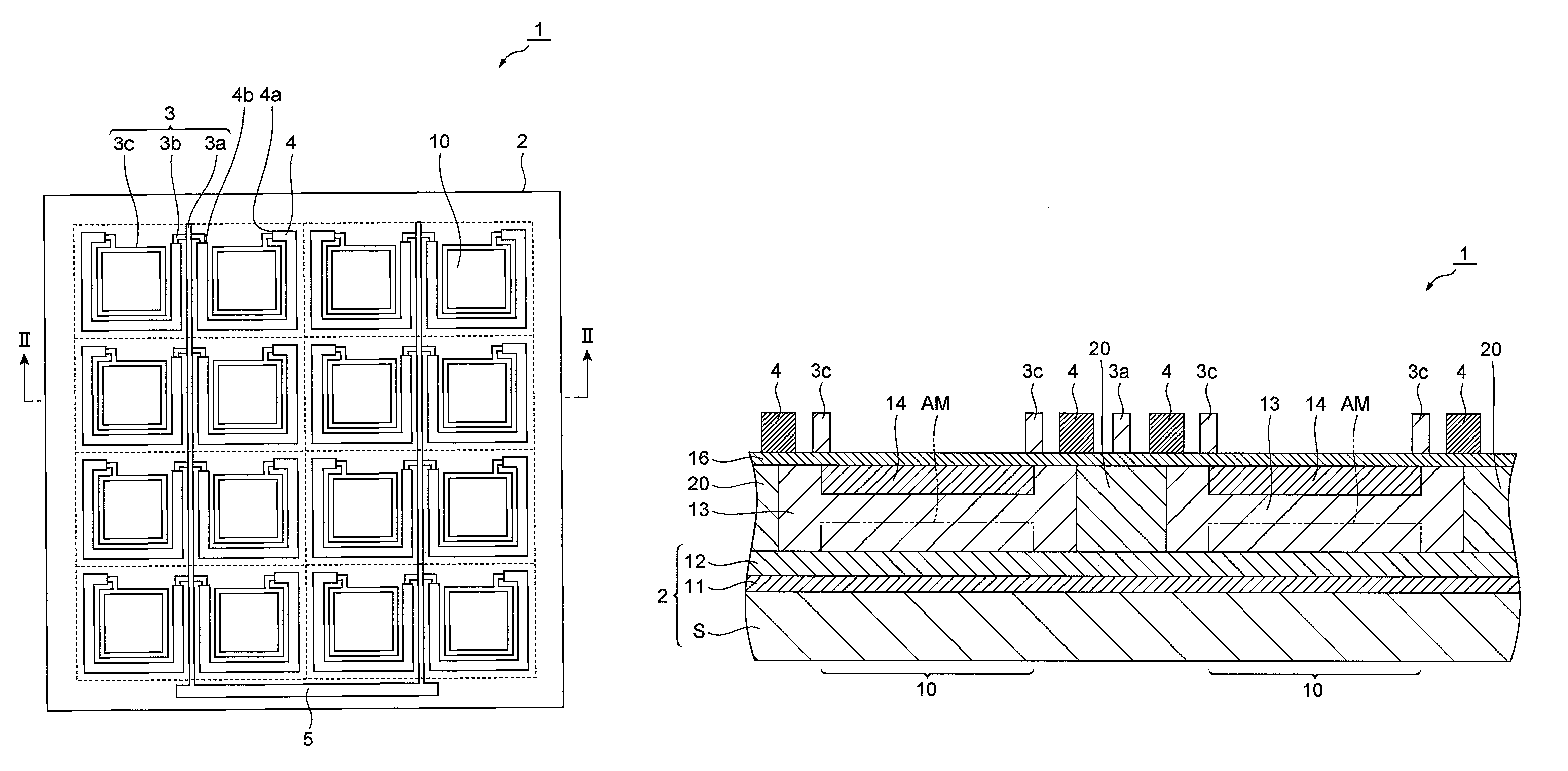
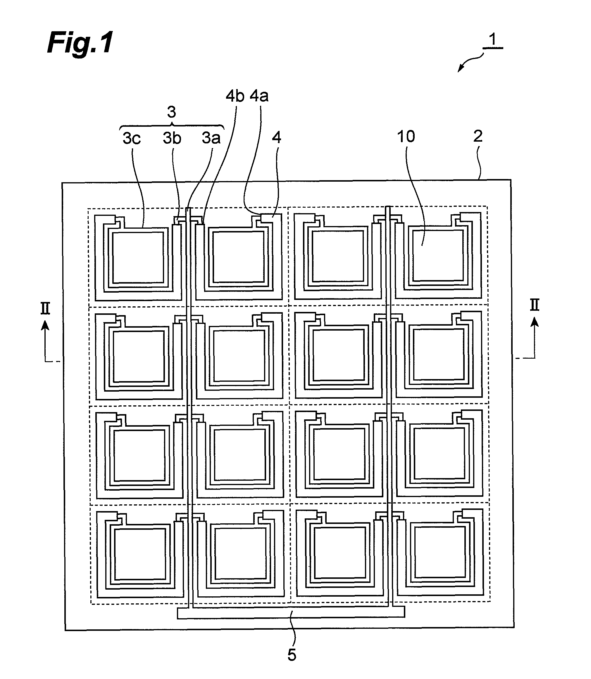
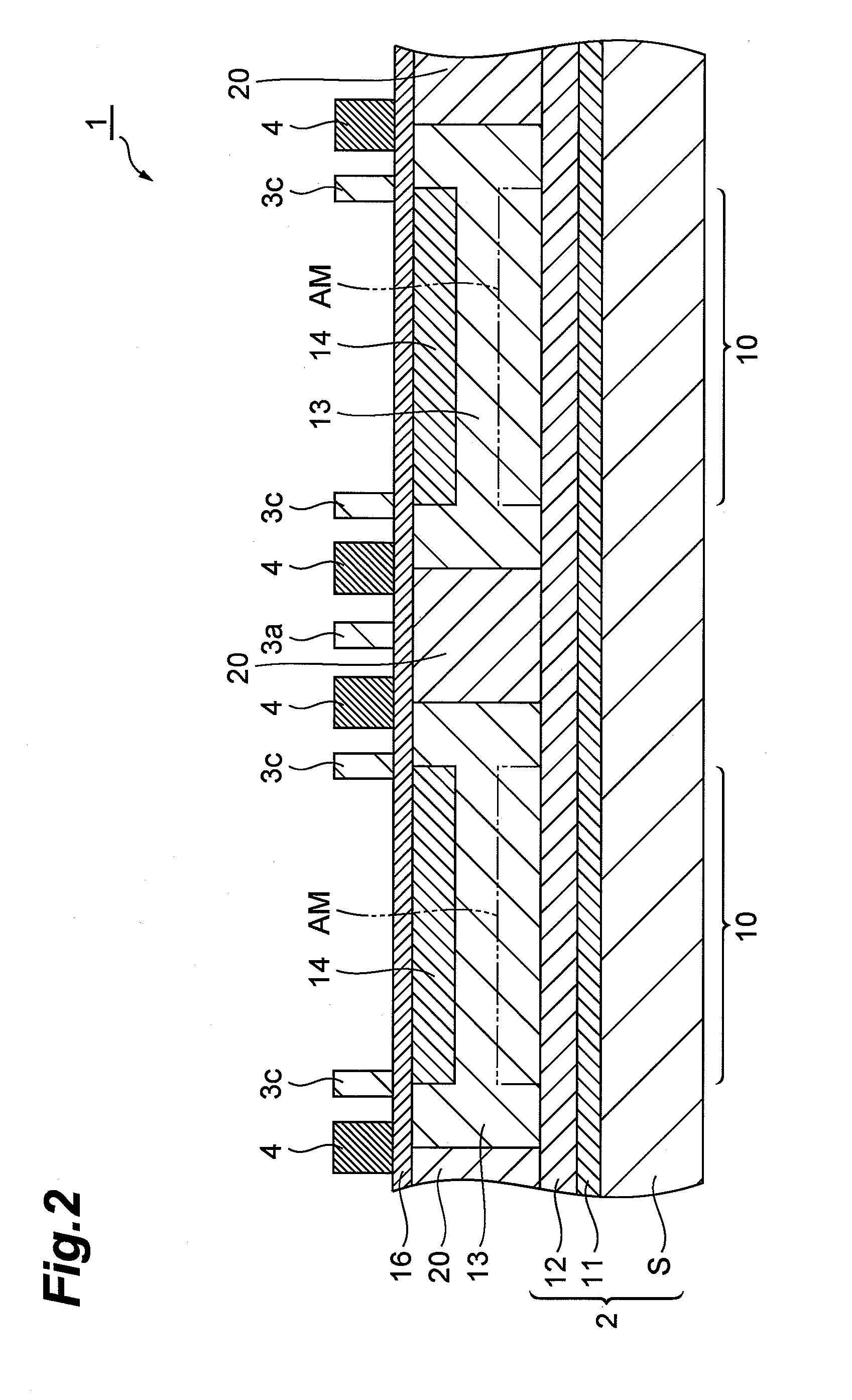
[0054]With reference to FIG. 1 and FIG. 2, the configuration of a photodiode array 1 according to a first embodiment will be explained below. FIG. 1 is a view schematically showing an upper surface of the photodiode array 1 according to a first embodiment. FIG. 2 is a view showing a part of the cross section taken along the line II-II of the photodiode array 1 according to the first embodiment.

[0055]The photodiode array 1 is formed with a plurality of semiconductor layers and an insulating layer laminated to a substrate 2. As shown in FIG. 1, the photodiode array 1 is a multichannel avalanche photodiode for photon counting having a plurality of photodetector channels 10 formed in a matrix (4×4 in the present embodiment) to which a light to be detected is incident. The photodiode array 1 has a signal conductor 3, resistors 4, and an electrode pad 5 on the upper surface thereof. The substrate 2 is a square with a side of about 1 mm, for example. Each of the photodetector channels 10 i...

second embodiment

[0077]With reference to FIG. 6, the configuration of a photodiode array 30 according to a second embodiment will be explained below. FIG. 6 is a view schematically illustrating the cross sectional structure of the photodiode array 30 according to the second embodiment. The photodiode array 30 according to the third embodiment is similar to the photodiode array 1 according to the first embodiment except that the separating part 20 has a light shielding part.

[0078]As shown in FIG. 6, the separating parts 20 comprises a light shielding part 22 formed of a material which absorbs a light of a wavelength band (from invisible to near infrared) which is to be detected by the photodetector channel 10. The light shielding part 22 is formed to be embedded in the separating part 20 like a core extending from the upper surface side to the lower surface side of the p−-type semiconductor layer 13. The light shielding part 22 is formed of a metal such as black photo-resist which is obtained by mixi...

third embodiment

[0088]With reference to FIG. 7, the configuration of a photodiode array 40 according to a third embodiment will be explained below. FIG. 7 is a view schematically illustrating the cross sectional structure of the photodiode array 40 according to a third embodiment. The photodiode array 40 according to the third embodiment is similar to the photodiode array 1 according to the first embodiment except that the signal conductor 3 is formed on a silicon nitride film.

[0089]As shown in FIG. 7, the photodiode array 40 comprises the substrate 2 having a semiconductor layer of n-type (a first conductivity type), the p-type semiconductor layer 15 of p-type (a second conductivity type) which is formed on the substrate 2, the p+-type semiconductor layer 14 of p-type which is formed on the p-type semiconductor layer 15, protective films 16a and 16b, the separating part 20 of n-type (the first conductivity type) formed on the p-type semiconductor layer 15, the signal conductor 3 formed of aluminum...


PUM


Abstract

A photodiode array 1 has a plurality of photodetector channels 10 which are formed on an n-type substrate 2 having an n-type semiconductor layer 12, with a light to be detected being incident to the plurality of photodetector channels 10. The photodiode array 1 comprises: a p−-type semiconductor layer 13 formed on the n-type semiconductor layer 12 of the substrate 2; resistors 4 each of which is provided to each of the photodetector channels 10 and is connected to a signal conductor 3 at one end thereof; and an n-type separating part 20 formed between the plurality of photodetector channels 10. The p−-type semiconductor layer 13 forms a pn junction at the interface between the substrate 2, and comprises a plurality of multiplication regions AM for avalanche multiplication of carriers produced by the incidence of the light to be detected so that each of the multiplication regions corresponds to each of the photodetector channels. The separating part 20 is formed so that each of the multiplication regions AM of the p−-type semiconductor layer 13 corresponds to each of the photodetector channels 10.

Description

TECHNICAL FIELD[0001]The present invention relates to a photodiode array.BACKGROUND ART[0002]In the fields of chemistry and medical care for example, there has been a technology for photon counting which uses a scintillator coupled with a photodiode array based on avalanche (electron avalanche) multiplication phenomenon. Such a photodiode array has divided photodetector channels formed on a common substrate in order to discriminate a plurality of photons which simultaneously enter thereto, and each of the photodetector channels is provided with multiplication regions (for example, see Non-Patent Documents 1 and 2, and Patent Document 1).[0003]Each multiplication region which is very sensitive to faint light is caused to be operated under an operation condition, called Geiger mode. That is, each multiplication region is applied with a reverse voltage that exceeds a breakdown voltage, and then the phenomenon is used in which carriers generated by the incident photons are multiplied in...

Claims


Application Information

Patent Timeline
Patent Type & Authority Patents(United States)
IPC IPC(8): H01L31/107
CPCH01L27/1446H01L27/14H01L31/107H01L27/14603H01L27/14605H01L27/14636
Inventor YAMAMURA, KAZUHISASATO, KENICHI
Owner HAMAMATSU PHOTONICS KK
Why Eureka
Try Eureka