Semiconductor structures

a technology of semiconductors and structures, applied in the direction of semiconductor devices, basic electric elements, electrical equipment, etc., can solve the problems of degrading the structural, morphological, electronic properties, stacking faults, point defects, etc., and achieve the effect of reducing the residual stress between the polycrystal substrate and the nucleation layer and reducing the density of dislocations

Active Publication Date: 2011-09-27
IND TECH RES INST
View PDF14 Cites 2 Cited by
  • Summary
  • Abstract
  • Description
  • Claims
  • Application Information

AI Technical Summary

Benefits of technology

[0009]During single crystal growth, dislocation density is reduced due to the lattice match between the polycrystal substrate and the nucleation layer. Additionally, due to their similar coefficients of thermal expansion (CTE), residual stress between the polycrystal substrate and the nucleation layer is effectively reduced when cooling subsequent to a high temperature process. Other defects such as stacking faults are also eliminated. Thus, a thick, high-purity single crystal layer is obtained.

Problems solved by technology

The layer contains structural defects such as point defects, misfit dislocations, and stacking faults.
These defects degrade the structural, morphological, and electronic properties of the film.

Method used


Image

  • Semiconductor structures
  • Semiconductor structures
  • Semiconductor structures

Examples


example 1

Preparation of Polycrystal Substrate I for Growth of Single Crystal Layer

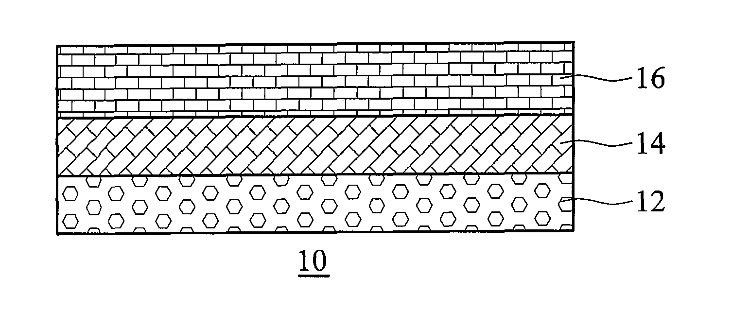
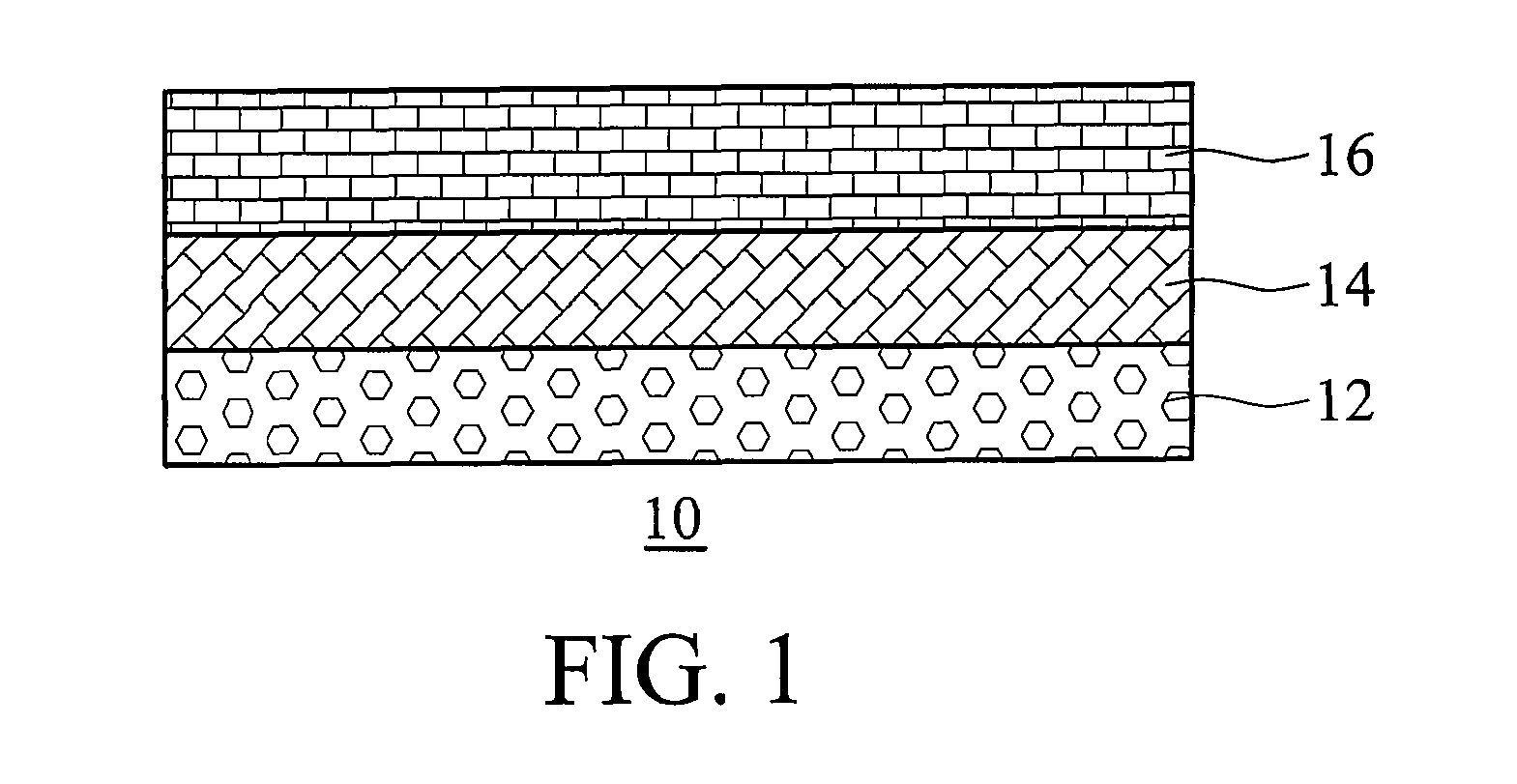
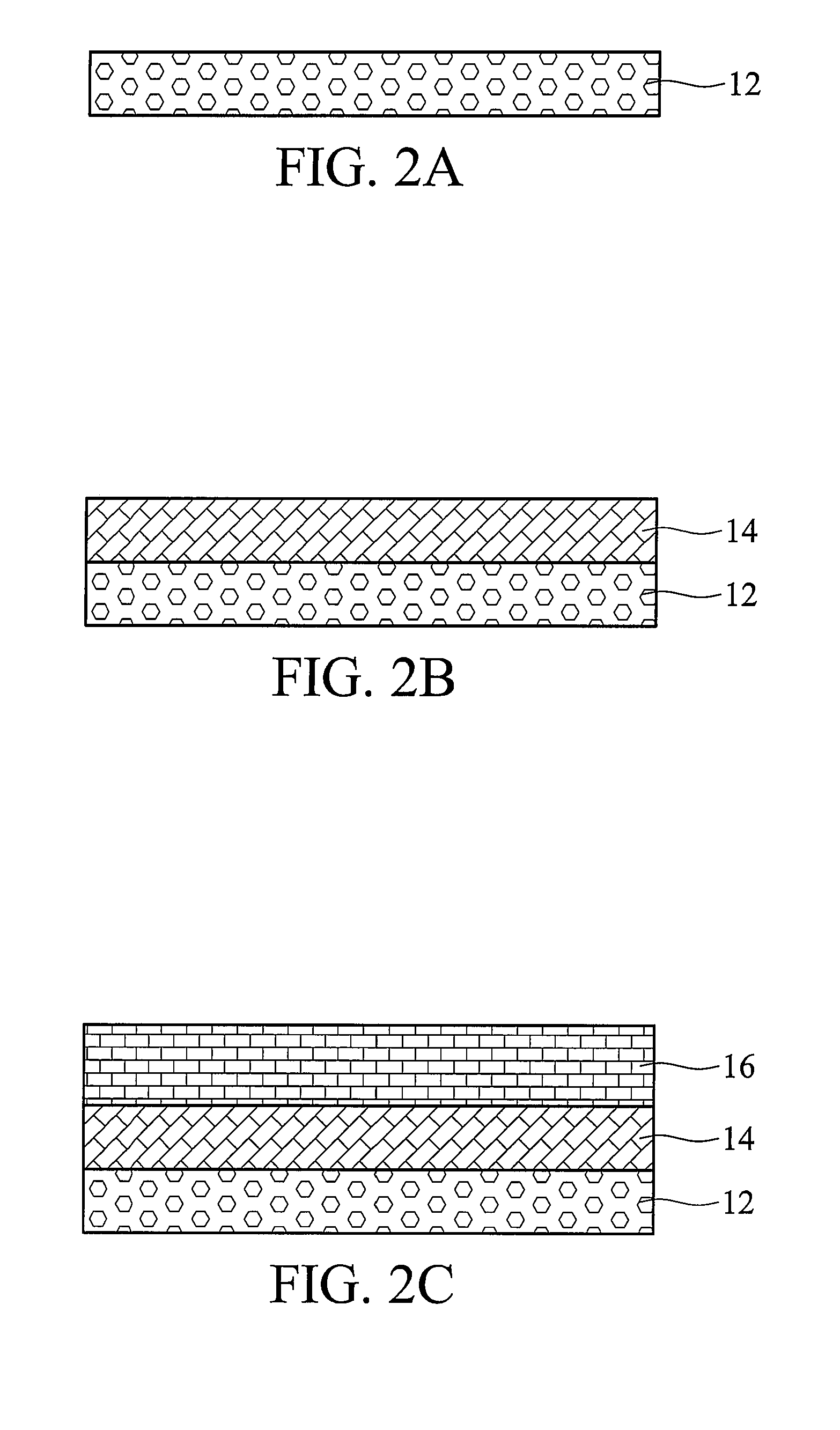
[0033]First, gallium oxide powders were shaped into a gallium oxide ceramic substrate. After CMP, the gallium oxide ceramic substrate was sintered in a nitrogen furnace to form a polycrystal gallium nitride substrate.

[0034]Next, a first single crystal gallium nitride layer obtained by the smart cut technique was transferred to the polycrystal gallium nitride substrate. The first single crystal gallium nitride layer was directly bonded on the polycrystal gallium nitride substrate.

[0035]After CMP, a second single crystal gallium nitride layer was grown on the first single crystal gallium nitride layer by metal organic chemical vapor deposition (MOCVD) process.

example 2

Preparation of Polycrystal Substrate II for Growth of Single Crystal Layer

[0036]First, gallium oxide powders were shaped into a polycrystal gallium oxide ceramic substrate. After CMP, a first single crystal gallium nitride layer obtained by the smart cut technique was transferred to the polycrystal gallium oxide substrate. The first single crystal gallium nitride layer was directly bonded on the polycrystal gallium oxide substrate.

[0037]After CMP, a second single crystal gallium nitride layer was grown on the first single crystal gallium nitride layer by metal organic chemical vapor deposition (MOCVD) process.

example 3

Preparation of Polycrystal Substrate III for Growth of Single Crystal Layer

[0038]First, gallium oxide powders were shaped into a gallium oxide ceramic substrate. After CMP, the surface of the gallium oxide ceramic substrate was treated with nitrogen to form a polycrystal gallium nitride layer with 0.3 μm. A composite polycrystal substrate comprising the bottom gallium oxide substrate and the upper gallium nitride layer was formed.

[0039]Next, a first single crystal gallium nitride layer obtained by the smart cut technique was transferred to the composite polycrystal substrate, directly bonded on the gallium nitride layer.

[0040]After CMP, a second single crystal gallium nitride layer was grown on the first single crystal gallium nitride layer by metal organic chemical vapor deposition (MOCVD) process.

[0041]The properties of the polycrystal substrates of the invention and the conventional substrates are compared in Table 1.

[0042]

TABLE 1coefficientsLatticeof thermalCrystalconstantexpans...


PUM


Abstract

A semiconductor structure is disclosed. The semiconductor structure includes a polycrystal substrate, a first single crystal layer formed thereon and a second single crystal layer formed on the first single crystal layer. A variation of coefficients of thermal expansion (CTE) between the first single crystal layer and the polycrystal substrate is less than 25%. There is no lattice mismatch between the first single crystal layer and the polycrystal substrate.

Description

BACKGROUND OF THE INVENTION[0001]1. Field of the Invention[0002]The invention relates to a semiconductor structure, and more particularly to a composite polycrystal substrate for growth of a single crystal layer.[0003]2. Description of the Related Art[0004]Recently, there has been enormous interest in the growth of Group III nitrides, and particularly gallium nitride (GaN) thin films, Jpn. J. Appl. Phys. Vol. 34 (1995) pp. L 797-L 799. GaN, and related (Aluminum, Indium) N alloys are being utilized for the production of efficient optoelectronic devices, such as, light emitters and detectors spanning the spectral range of visible to deep ultra-violet (UV) light. The direct, wide bandgap and the chemical stability of Group III nitrides are very beneficial for high-temperature and high-power electronic devices, such as, hetero-junction bipolar and field effect transistors.[0005]When GaN is directly grown on a sapphire substrate, the growth mode is three-dimensional due to the large lat...

Claims


Application Information

Patent Timeline
Patent Type & Authority Patents(United States)
IPC IPC(8): H01L29/04
CPCH01L21/187
Inventor CHIU, KUO-CHUANGLIN, TZER-SHEN
Owner IND TECH RES INST
Why Eureka
Try Eureka