Wafer level package integrated circuit incorporating solder balls containing an organic plastic-core

a solder ball and integrated circuit technology, applied in the direction of electrical apparatus, semiconductor devices, semiconductor/solid-state device details, etc., can solve the problems of permanent damage to the integrated circuit, stress around the region of the substrate, etc., to achieve effective absorption of forces, good elongation properties, and high resistance

Active Publication Date: 2011-10-11
MAXIM INTEGRATED PROD INC
View PDF3 Cites 53 Cited by
  • Summary
  • Abstract
  • Description
  • Claims
  • Application Information

AI Technical Summary

Benefits of technology

[0005]An aspect of the invention relates to using solder balls containing an elastic or resilient material core, a hard or rigid shell substantially enclosing the core, and an electrical contact layer substantially enclosing the shell. The elastic or resilient core serves as a stress buffer layer in a wafer level package (WLP) integrated circuit. Each elastic or resilient material core may include an organic-plastic material, such as Divinilbenzene cross-linked co-polymer of relatively high resistance. It has a relatively good elongation property so that it can effectively absorb forces exerted on the integrated circuit by, for example, the flexing of a printed circuit board (PCB) or other structure to which the integrated circuit is attached. The organic-plastic material also has a relatively high strength property to protect the integrated circuit from external forces. Thus, the solder balls can further assist in effectively protecting the integrated circuit during manufacturing, handling, and operation.

Problems solved by technology

However, the bending of the flexible substrate creates stress around the region where the solder balls attach to the integrated circuit.
Sometimes the stress causes permanent damage to the integrated circuit.

Method used


Image

  • Wafer level package integrated circuit incorporating solder balls containing an organic plastic-core
  • Wafer level package integrated circuit incorporating solder balls containing an organic plastic-core
  • Wafer level package integrated circuit incorporating solder balls containing an organic plastic-core

Examples


Embodiment Construction

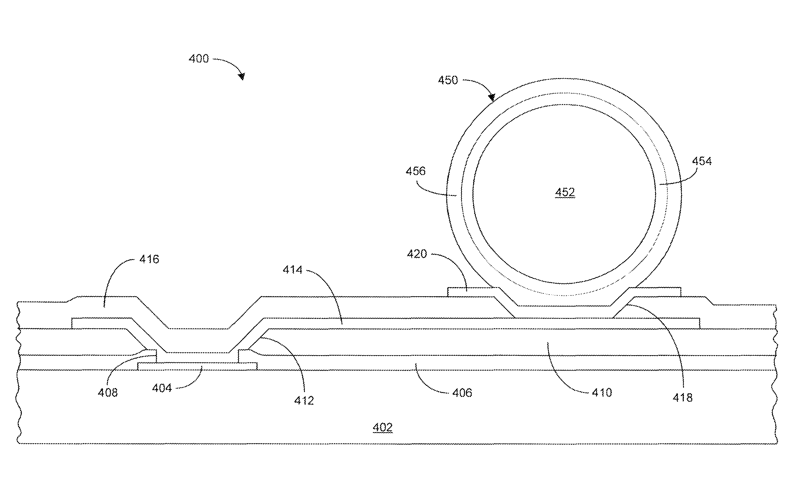
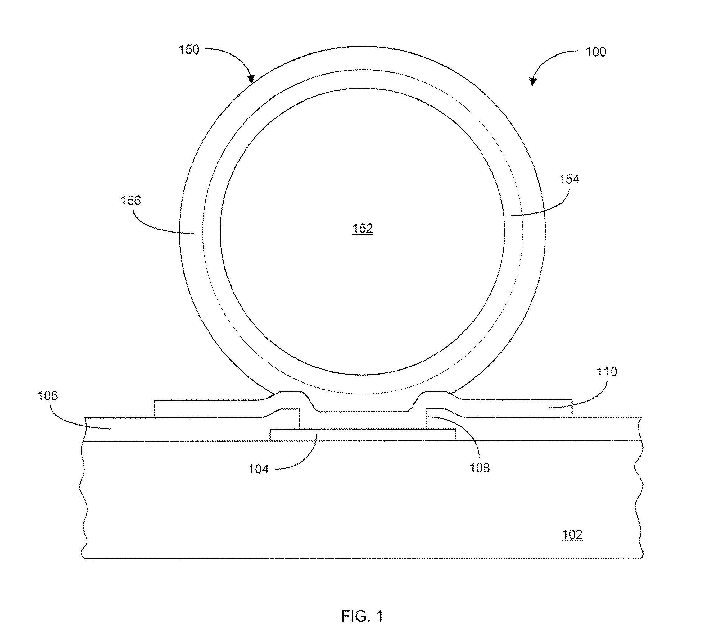
[0017]FIG. 1 illustrates a sectional view of an exemplary integrated circuit 100 in accordance with an embodiment of the invention. The integrated circuit 100 is an example of a bump on pad (BOP) implementation having a solder ball with an organic-plastic core that serves as a stress buffer layer. In this example, a single bond pad and respective solder bump are used to exemplify the invention. It shall be understood that the integrated circuit 100 may have a plurality of bond pads and respective solder balls in the configuration described herein.

[0018]In particular, the integrated circuit 100 comprises a semiconductor substrate 102 (e.g., a silicon substrate) including one or more active devices. The integrated circuit 100 further comprises at least one bond pad 104 for electrically connecting the integrated circuit to external components. The bond pad 104 is disposed over the substrate 102, and may comprise any suitable electrical conductor, such as aluminum, copper, aluminum allo...


PUM


Abstract

An integrated circuit including solder balls containing an elastic or resilient material core, a hard or rigid shell substantially enclosing the core, and an electrical contact layer substantially enclosing the shell. The elastic or resilient core serves as a stress buffer layer in a wafer level package (WLP) integrated circuit. The elastic or resilient material core may include an organic plastic material, such as a Divinilbenzene cross-linked co-polymer of relatively high resistance. This material has a relatively good elongation property so that it can effectively absorb forces exerted upon the integrated circuit by, for example, the flexing of a printed circuit board (PCB) or other structure to which the integrated circuit is attached. The hard or rigid shell serves to contain the elastic or resilient core and may include copper. The electrical contact layer serve to provide a good adhesive electrical contact to an under bump metallization (UBM) layer, may include a lead free, Tin-Gold (SnAg) material.

Description

FIELD OF THE INVENTION[0001]This invention relates generally to integrated circuits, and in particular, to an integrated circuit comprising solder balls including an organic plastic-core that serves as a stress buffer layer in wafer level package (WLP) integrated circuits.BACKGROUND OF THE INVENTION[0002]Integrated circuits are continuously undergoing development to provide smaller footprints while providing the same or higher circuit densities. Additionally, the packaging of integrated circuit is also continuously undergoing development to provide packages only slightly larger than the integrated circuits they are housing. For instance, integrated circuit packages using wire bonds connected to a lead frame, that typically require a relatively large footprint, are generally being replaced with chip scale packages (CSP), such as wafer level packages (WLP), wherein the size of the package is substantially the same or slightly larger than the integrated circuit it houses.[0003]In a typ...

Claims


Application Information

Patent Timeline
Patent Type & Authority Patents(United States)
IPC IPC(8): H01L23/48
CPCH01L23/3192H01L24/05H01L24/13H01L2924/0002H01L2224/02381H01L2224/0239H01L2224/024H01L2224/0401H01L2224/05571H01L2224/05572H01L2224/05624H01L2224/05647H01L2224/1319H01L2224/13561H01L2224/13582H01L2224/13611H01L2224/13639H01L2224/13647H01L2924/01013H01L2924/01029H01L2924/01079H01L2924/01082H01L2924/014H01L2924/01023H01L2924/01033H01L2924/01047H01L2924/0105H01L2924/01074H01L2224/05552H01L2924/351H01L2924/14H01L2224/05569H01L2224/05008H01L2924/00
Inventor WILCOXEN, DUANE T.BOJKOV, CHRISTO P.GHAI, AJAY KUMARCATE, STEVE DETLEV
Owner MAXIM INTEGRATED PROD INC
Why Eureka
Try Eureka