Procedure for obtaining nanotube layers of carbon with conductor or semiconductor substrate

a technology of conductors and semiconductor substrates, applied in the direction of liquid/solution decomposition chemical coating, solid/suspension decomposition chemical coating, superimposed coating process, etc., can solve the problem that the growth process is unsuitable for producing interconnections in an integrated circui

Active Publication Date: 2011-10-18
COMMISSARIAT A LENERGIE ATOMIQUE ET AUX ENERGIES ALTERNATIVES
View PDF10 Cites 0 Cited by
  • Summary
  • Abstract
  • Description
  • Claims
  • Application Information

AI Technical Summary

Problems solved by technology

The presence of an oxide layer makes the aforementioned growth processes unsuitable for producing interconnections in an integrated circuit.

Method used


Image

  • Procedure for obtaining nanotube layers of carbon with conductor or semiconductor substrate
  • Procedure for obtaining nanotube layers of carbon with conductor or semiconductor substrate
  • Procedure for obtaining nanotube layers of carbon with conductor or semiconductor substrate

Examples


example 1

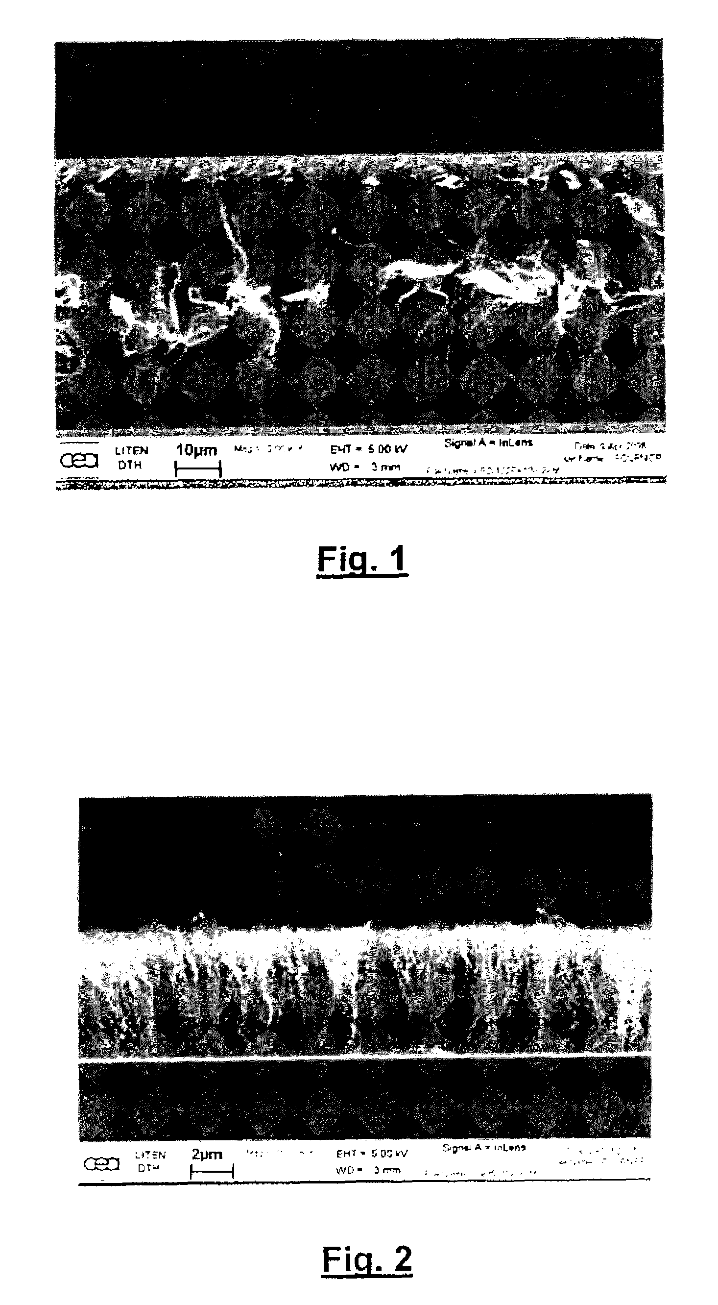
[0051]The substrate used was single-crystal silicon deoxidized by argon ion bombardment. The catalytic system consisted of a 1 nm layer of iron deposited on the deoxidized silicon by means of argon ion beam sputtering.

[0052]The iron layer then underwent an oxidizing plasma treatment with two successive air plasmas generated at room temperature and at a pressure of 0.4 mbar.

[0053]The specimen was placed on the electrode connected to the RF source.

[0054]The first plasma with relatively high energy induced a 120 V self-bias voltage on the specimen, enabling it to be bombarded while oxidizing it.

[0055]The second plasma with a relatively lower energy induced a 65 V self-bias voltage.

[0056]Once the oxidizing treatment had been completed, the specimen was heated to a temperature of 560° C. under a hydrogen partial pressure of 0.2 mbar.

[0057]The nanotubes were grown by then introducing a gas mixture consisting of acetylene, helium and hydrogen, with respective flow rates of 10 standard cm3 / ...

example 2

[0060]This example is identical to the previous one except for the type of deposition of the iron layer. After wet etching of the silicon with hydrofluoric acid, the iron layer was deposited by electron-beam evaporation. The rest of the growth process was identical to that of Example 1. The results obtained are similar to those obtained previously.

example 3

[0061]The substrate used was a titanium nitride (TiN) layer. The catalytic system consisted here of a 2 nm iron layer on a 5 nm amorphous silicon layer. The amorphous silicon layer and then the iron layer were deposited by means of ion beam sputtering during the same vacuum cycle.

[0062]An oxidizing plasma treatment was then carried out, under the same conditions as those in Example 1, followed by growth of the nanotubes.

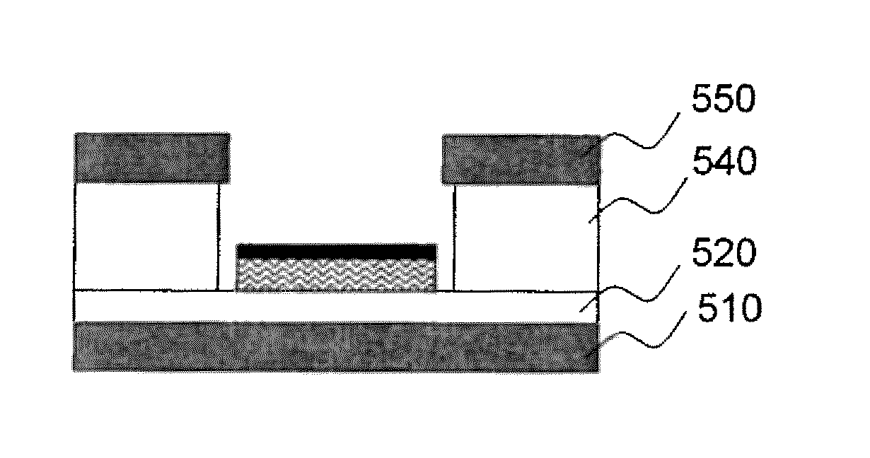
[0063]Under these conditions, a dense mat of nanotubes on TiN, having a length of 32 μm and a density of 2×1011 cm−2, as illustrated in FIG. 3, was obtained.

[0064]FIG. 4 shows by comparison the case in which a single iron layer is deposited on the TiN layer without prior oxidizing treatment. The absence of nanotube growth on this layer is therefore observed.

[0065]The process for producing a CTN mat according to the invention may be used for the production of interconnect elements, especially vias in an integrated circuit.

[0066]FIGS. 5A to 5H show the various steps in...


PUM

PropertyMeasurementUnit
thicknessaaaaaaaaaa
thicknessaaaaaaaaaa
temperatureaaaaaaaaaa

Abstract

The present invention relates to a process for producing a carbon nanotube (CNT) mat on a conductive or semiconductor substrate. According to this process, a catalytic complex comprising at least one metal layer is firstly deposited on said substrate. Said metal layer then undergoes an oxidizing treatment. Finally, carbon nanotubes are grown from the metal layer thus oxidized. The present invention also relates to a process for producing a via using said CNT mat production process.

Description

TECHNICAL FIELD[0001]The present invention relates to the field of carbon nanotubes. It is particularly applicable for the production of vias in integrated circuits.PRIOR ART[0002]The use of nanotubes for interconnecting various layers of an integrated circuit has recently been the subject of considerable research. Their excellent conducting properties and their electrical and thermal stability mean that carbon nanotubes (CNTs) are excellent candidates for producing vias of very small diameter. An example of a CNT-derived via is described in Application WO 01 / 61753.[0003]One essential characteristic of a via is its electrical resistance which, when it is based on CNTs, depends on the density of the nanotubes per unit area. In practice, the CNT mat in the via must reach a nanotube density of the order of 1011 to 1013 cm−2 in order to have an electrical resistance comparable to that of copper. These nanotubes must be connected to the semiconductor substrate or to a conductive layer de...

Claims


Application Information

Patent Timeline
Patent Type & Authority Patents(United States)
IPC IPC(8): H01L21/20
CPCB82Y30/00H01L21/76843H01L21/76856H01L21/76876H01L21/76879H01L23/53276H01L2221/1094Y10S977/855H05K3/4038H01L2924/0002Y10S977/742Y10S977/70H01L2924/00
Inventor DIJON, JEANFOURNIER, ADELINE
Owner COMMISSARIAT A LENERGIE ATOMIQUE ET AUX ENERGIES ALTERNATIVES
Why Eureka
Try Eureka