Supercharge Your Innovation With Domain-Expert AI Agents!

Hybrid semiconductor substrate including semiconductor-on-insulator region and method of making the same

a hybrid semiconductor and substrate technology, applied in the direction of semiconductor devices, basic electric elements, electrical apparatus, etc., can solve the problems of increased process cost and time for fabrication, significant instabilities of devices, and increase in process cost and time, so as to achieve sram stability, suppress threshold voltage (vt) fluctuations, and achieve the effect of sram stability

Active Publication Date: 2011-11-15
SOITEC SA
View PDF6 Cites 10 Cited by
  • Summary
  • Abstract
  • Description
  • Claims
  • Application Information

AI Technical Summary

Benefits of technology

This approach simplifies the manufacturing process, reduces costs, and improves SRAM stability by suppressing threshold voltage fluctuations in SeOI regions, enabling simultaneous creation of back side electrodes and channels in transistors.

Problems solved by technology

In particular, for static random access memory (SRAM) cells, the threshold voltage fluctuations may result in significant instabilities of the devices, which may not be tolerable in view of data integrity of the memory cells.
The process cost and time for the fabrication thus increases due to the need of a plurality of different masks to be able to carry out the implant steps in both the SeOI region and the bulk semiconductor region and, thereby, a greater number of process steps.

Method used


Image

  • Hybrid semiconductor substrate including semiconductor-on-insulator region and method of making the same
  • Hybrid semiconductor substrate including semiconductor-on-insulator region and method of making the same
  • Hybrid semiconductor substrate including semiconductor-on-insulator region and method of making the same

Examples


first embodiment

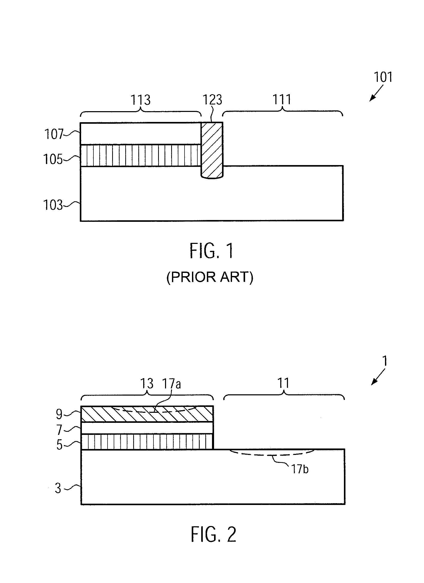
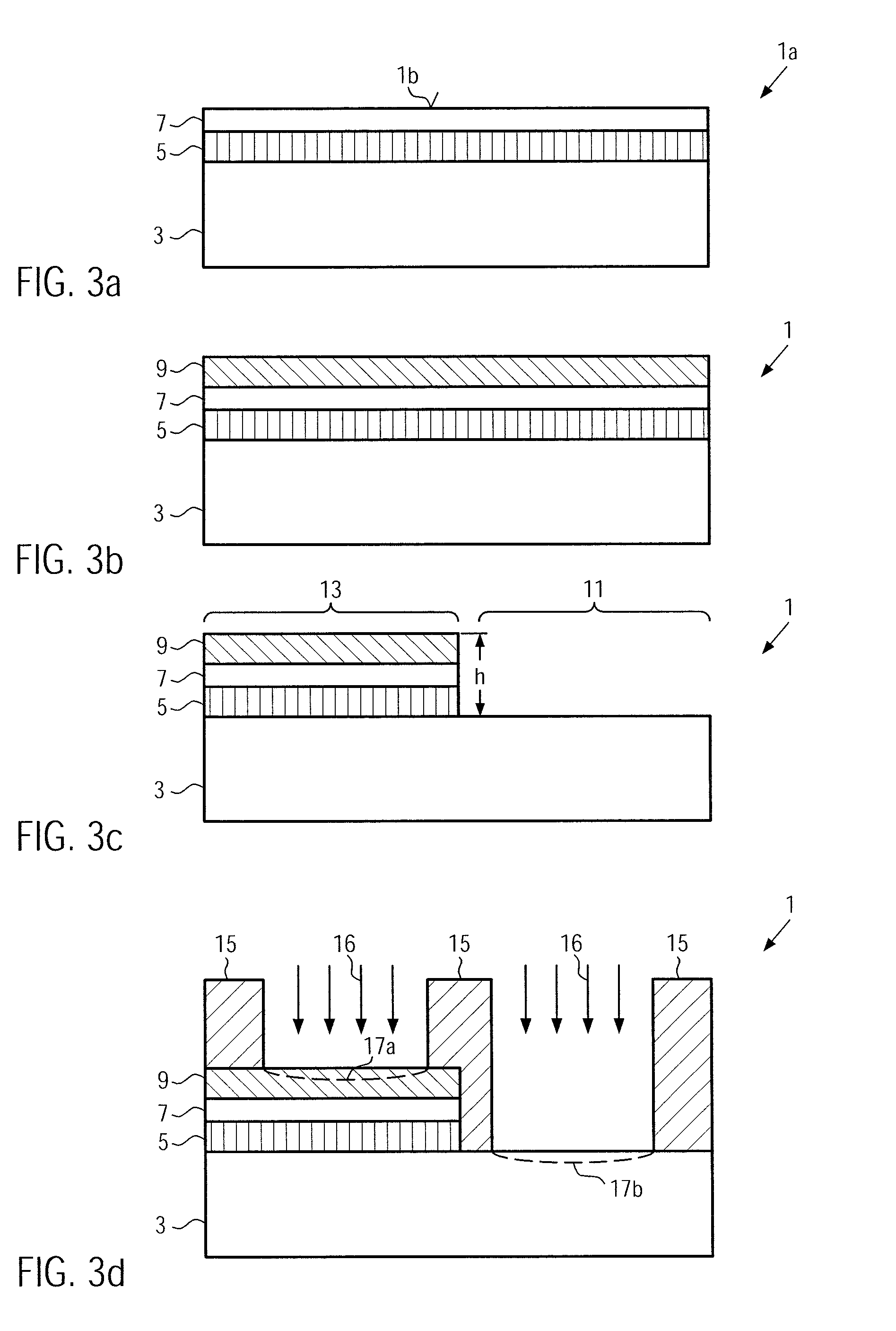
[0036]FIG. 2 illustrates a hybrid semiconductor substrate 1 according to the invention. The fabrication method to manufacture the hybrid semiconductor substrate 1 will be described with respect to FIGS. 3a-3d.

[0037]The hybrid semiconductor substrate 1 comprises a base substrate 3 with a semiconductor-on-insulator (SeOI) region 13 that comprises an insulating layer 5, a semiconductor layer 7 also called a SeOI layer, and a mask layer 9.

[0038]The hybrid semiconductor substrate 1 furthermore comprises a bulk semiconductor region 11 adjacent to the SeOI region 13 and that shares the same base substrate 3.

[0039]In this embodiment, the base substrate 3 is a Si wafer, the insulating layer 5 is a silicon oxide layer, also called a buried oxide layer (BOX), and the SeOI layer 7 is a silicon containing layer. The material choice is nevertheless non-limiting and other suitable materials, like germanium, gallium, arsenide, etc., may find application for the substrate 3 and the SeOI layer 7. Re...

second embodiment

[0067] the inventive method for manufacturing the hybrid semiconductor substrate 1 comprises a step of providing a spacer 29 in an edge region of the SeOI region 13 adjacent to the bulk semiconductor region 11, as illustrated in FIG. 4c. The spacer 29 extends at least from the surface of the base substrate 3 to an interface 31 between the SeOI layer 7 and the mask layer 9.

[0068]The spacer 29 protects the SeOI layer 7 and the insulating layer 5 of the SeOI region 13 from damage while the mask layer 9 is removed from the hybrid semiconductor substrate 1, e.g., by etching, during the step (h) illustrated in FIG. 3g and FIG. 4g.

[0069]According to this embodiment, the spacer 29 is a nitride. A nitride is one example of a suitable material to protect the insulating layer 5 during etching of the mask layer 9, as it has different etching properties compared to the oxide used for the mask layer 9 and the insulating layer 5. This effect is thus achieved for any material choice for the spacer...


PUM


Abstract

A method for manufacturing a hybrid semiconductor substrate comprises the steps of (a) providing a hybrid semiconductor substrate comprising a semiconductor-on-insulator (SeOI) region, that comprises an insulating layer over a base substrate and a SeOI layer over the insulating layer, and a bulk semiconductor region, wherein the SeOI region and the bulk semiconductor region share the same base substrate; (b) providing a mask layer over the SeOI region; and (c) forming a first impurity level by doping the SeOI region and the bulk semiconductor region simultaneously such that the first impurity level in the SeOI region is contained within the mask. Thereby, a higher number of process steps involved in the manufacturing process of hybrid semiconductor substrates may be avoided.

Description

PRIORITY CLAIM[0001]This application claims the benefit of the filing date of European Patent Application Serial No. EP 09290372.3, filed May 18, 2009 and entitled “Fabrication Process of a Hybrid Semiconductor Substrate,” which is incorporated herein in its entirety by this reference.TECHNICAL FIELD[0002]The present invention relates to a fabrication process of a hybrid semiconductor substrate, and more particularly, relates to simultaneous fabrication of hybrid semiconductor substrates.BACKGROUND[0003]A semiconductor device, in which a semiconductor-on-insulator (SeOI) region and a bulk semiconductor region are formed on an upper surface of a semiconductor base substrate, wherein the SeOI region comprises a buried insulating oxide layer (BOX) and a thin semiconductor layer, is known as a hybrid semiconductor device. Such a device may be used in memory cell.[0004]FIG. 1 is a cross-sectional view of a known hybrid semiconductor device 101 like, for example, disclosed in Yamaoka et a...

Claims


Application Information

Patent Timeline
Patent Type & Authority Patents(United States)
IPC IPC(8): H01L21/425H01L21/70
CPCH01L21/187H01L21/2007H01L27/1207H01L21/823412H01L21/823481H01L21/26513H01L21/762
Inventor BOURDELLE, KONSTANTINNGUYEN, BICH-YENSADAKA, MARIAM
Owner SOITEC SA
Features
  • R&D
  • Intellectual Property
  • Life Sciences
  • Materials
  • Tech Scout
  • Unparalleled Data Quality
  • Higher Quality Content
  • 60% Fewer Hallucinations
Learn More