

Composite field emission source
a composite field and emission source technology, applied in the manufacture of electric discharge tubes/lamps, electrode systems, discharge tubes luminescnet screens, etc., can solve the problems of difficult control of emission current, carbon nanotube structure cannot bear high current, easy to be burnt up, etc., to reduce the turn-on field, increase the amount of carbon accumulation, and increase the strength of the composite field emission source
- Summary
- Abstract
- Description
- Claims
- Application Information
AI Technical Summary
Benefits of technology
Problems solved by technology
Method used
Image

Examples
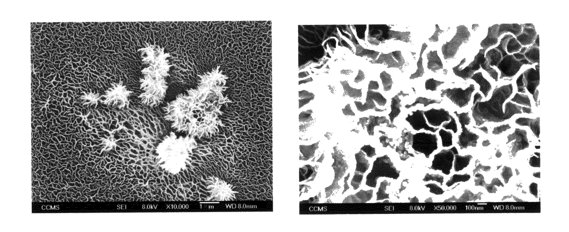
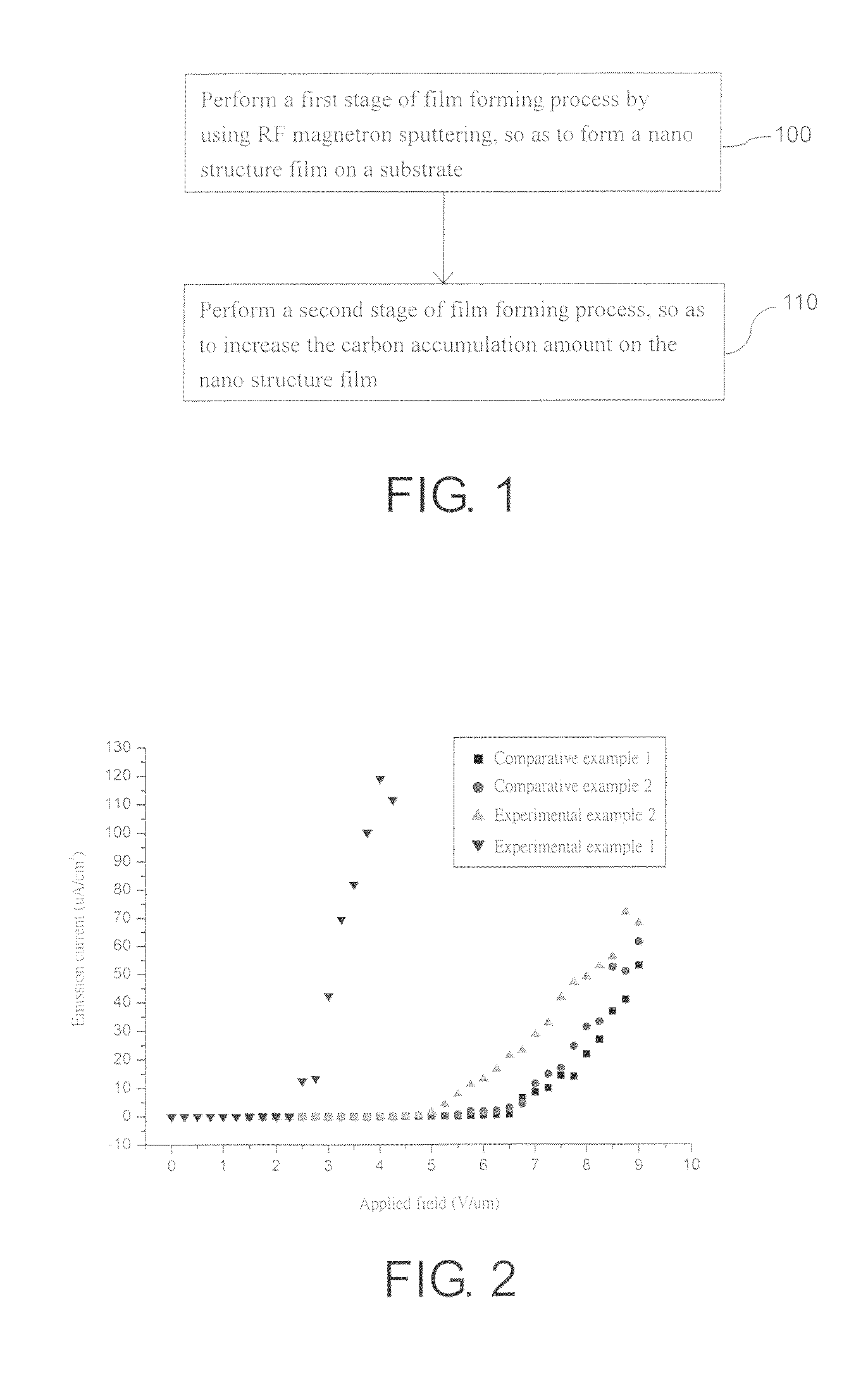
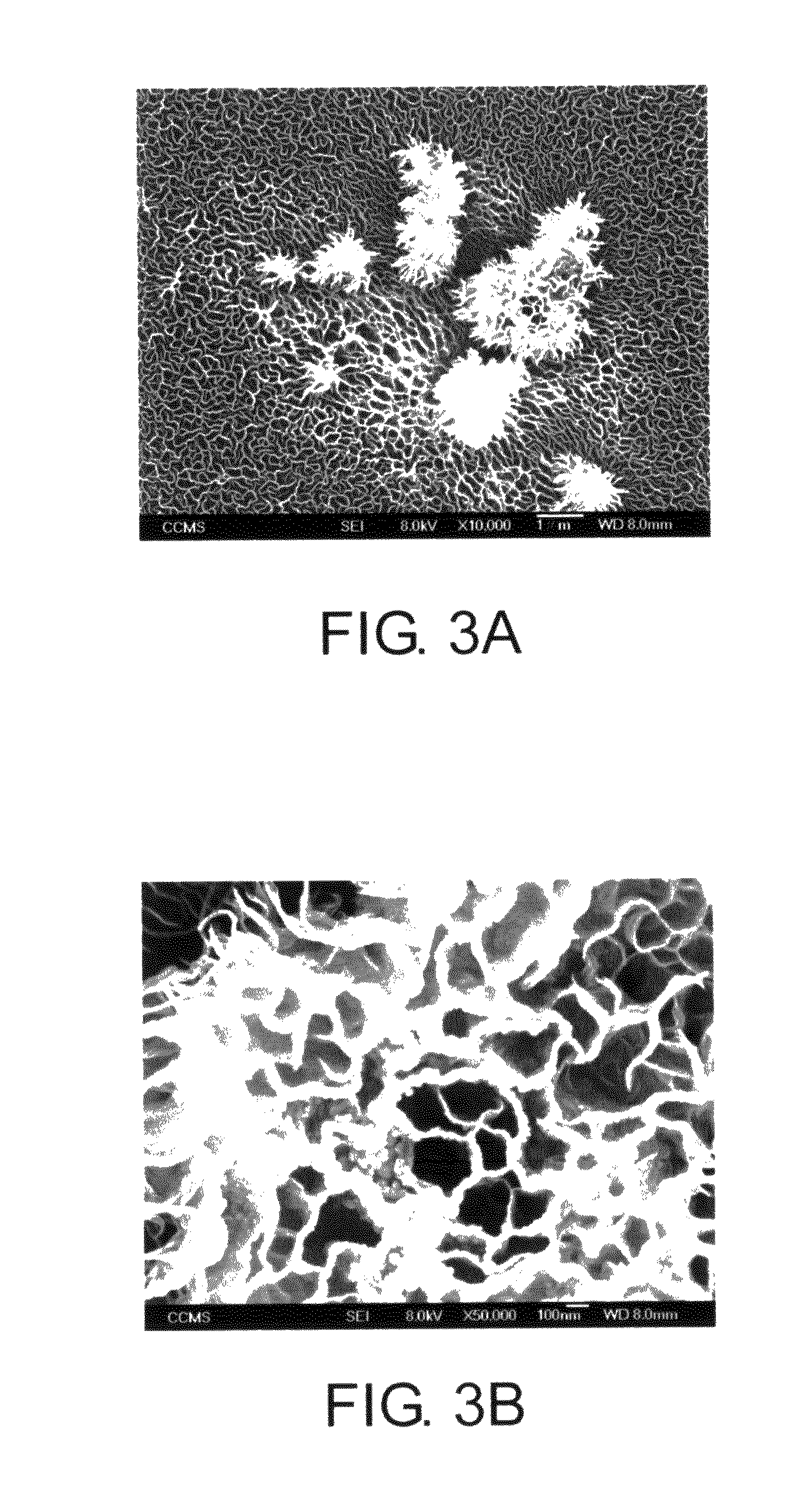
experimental example 1
[0038]After being cleaned, a silicon substrate is placed in a reactive RF magnetron sputtering system, and the temperature is controlled at 375° C. Then, gases required by the reaction are provided with controlled flow. In the experimental example 1, the provided gases are respectively Ar, H2, and CH4, and a gas flow ratio is 5:3:2.5. At the same time, the pressure is controlled at 10 mtorr. Then, a sputtering reaction is performed on the surface of the substrate for 50 minutes with a RF power 100 W, such that a nano structure film is grown on the surface of the silicon substrate.
[0039]Next, the silicon substrate grown with the nano structure film is moved into a furnace tube, the temperature of the furnace tube is controlled at 800° C., and then NH3 and C2H2 are provided, in which the gas flows are respectively 100 sccm and 30 sccm. At the same time, the pressure is controlled at 3 torr, such that the thermal CVD reaction is performed on the substrate for 10 minutes, so as to incre...
experimental example 2
[0040]After the surface of a silicon substrate is cleaned, the first stage of film-forming process is finished by using the reactive RF magnetron sputtering system and processing parameters identical to those of the [Experimental Example 1]. Then, the second stage of film-forming process is performed by using RF magnetron sputtering, in which the temperature is controlled to be higher than or equal to 400° C.
PUM
| Property | Measurement | Unit |
|---|---|---|
| temperature | aaaaa | aaaaa |
| temperature | aaaaa | aaaaa |
| temperature | aaaaa | aaaaa |
Abstract
Description
Claims
Application Information