
Method of molding glass parts and molding apparatus

a molding apparatus and glass material technology, applied in glass rolling apparatus, blowing machines, instruments, etc., can solve the problems of increasing the size of pressure means, increasing the molding area, and low processing efficiency of glass materials in processing employing semiconductor processes such as dry-etching, so as to improve the life of molding dies and resist oxidizing atmosphere.

Inactive Publication Date: 2012-01-24
NAT INST OF ADVANCED IND SCI & TECH
View PDF23 Cites 45 Cited by
  • Summary
  • Abstract
  • Description
  • Claims
  • Application Information

AI Technical Summary

Benefits of technology

The present invention relates to a technology for processing glass materials using a micromolding process. The invention aims to solve the problem of low processing efficiency for glass materials using traditional semiconductor processes. The invention proposes a micromolding technology employing a molding die for replicating a profile by pressing the molding die against the glass material at a high temperature. However, there are challenges in applying this technology to large-area glass materials, such as difficulty in uniform application of pressure, increased size of the molding apparatus, and burden on the molding die. The invention proposes a solution to these challenges by developing a load means employing a fluid as a medium and a method for scanning the entire area to be molded with a small pressure head. The invention also addresses the issue of cracking of the molding die by proposing a method for reducing the load on the die during the molding process.

Problems solved by technology

However, processing employing a semiconductor process such as dry-etching has a low processing efficiency for the glass material.
Increase in area of molding is also an important issue for increasing a speed and an efficiency of a molding step.
Therefore, a pressure means is extremely increased in size, which in turn results in remarkably increased size of a molding apparatus.
In addition, it becomes difficult to uniformly apply a pressure to a region to be molded.
However, there is a problem that various additive elements contained in the low-melting-point glass affect optical performance or chemical stability.
Thus, there is a problem that the apparatus is increased in size.
Moreover, the glass requires a larger pressure for molding as compared with that required for the resin material, and hence means for applying a large load is required.
Therefore, there also arises a problem that the apparatus becomes large.
However, a weight uniformization means using the fluid as the medium or the like cannot be used at a high temperature.
Moreover, the application of the scanning method with the pressure head is also difficult in view of heat shield of the entire mechanism and the accommodation of the mechanism in a vacuum chamber.
Therefore, for molding of the glass material over a large area, the apparatus becomes extremely large in size and expensive.
Further, a burden imposed on the molding die becomes large in the molding under the conditions of a high temperature and a large load.
Thus, the cracking of the molding die also becomes a problem.[Non-Patent Literature 1]“Nanostructure Fabrication by Nanoimprint Technology” by Hirai, Journal of the Japan Society for Precision Engineering, vol.

Method used


Image

  • Method of molding glass parts and molding apparatus
  • Method of molding glass parts and molding apparatus
  • Method of molding glass parts and molding apparatus

Examples


example 1

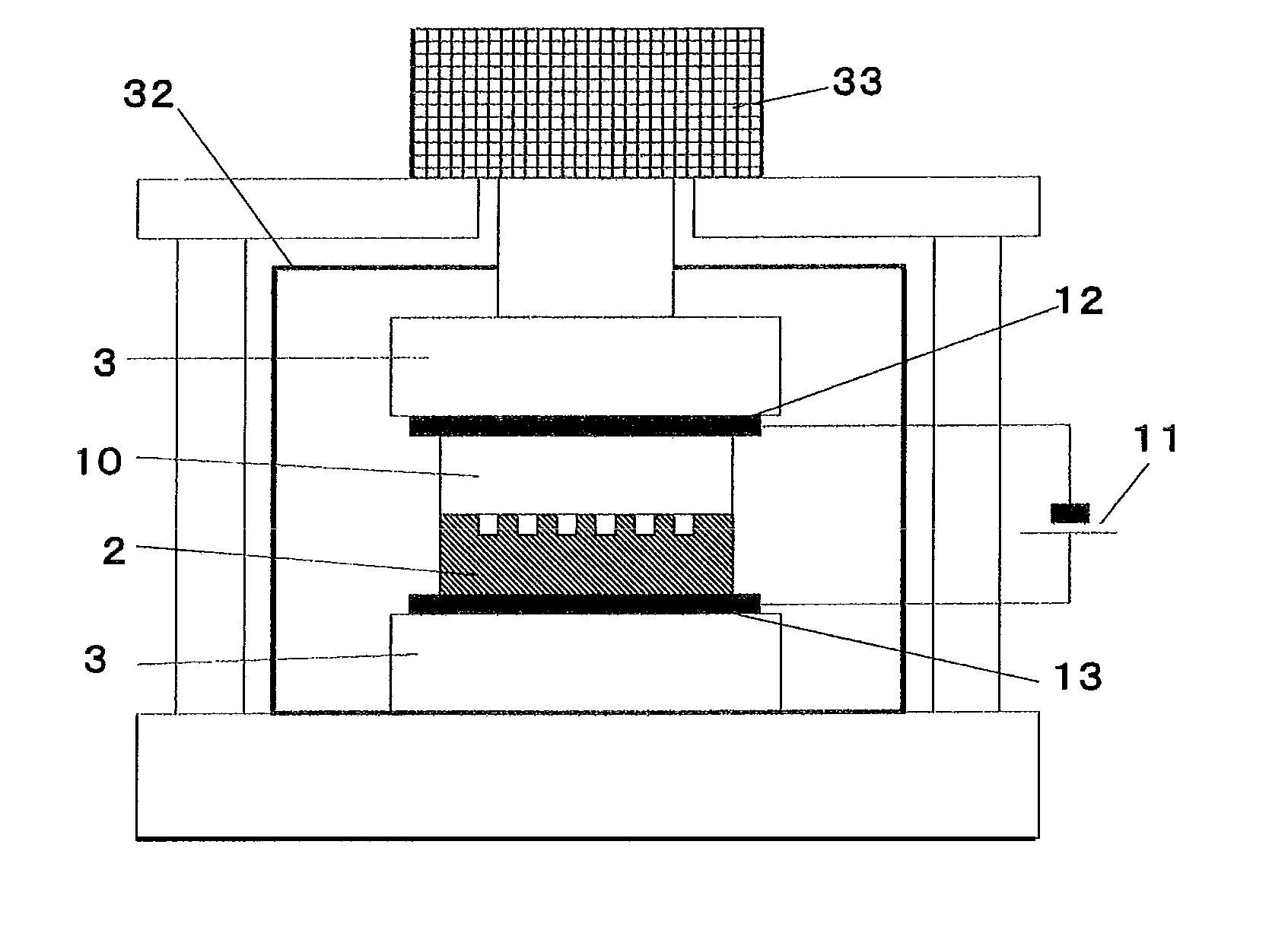
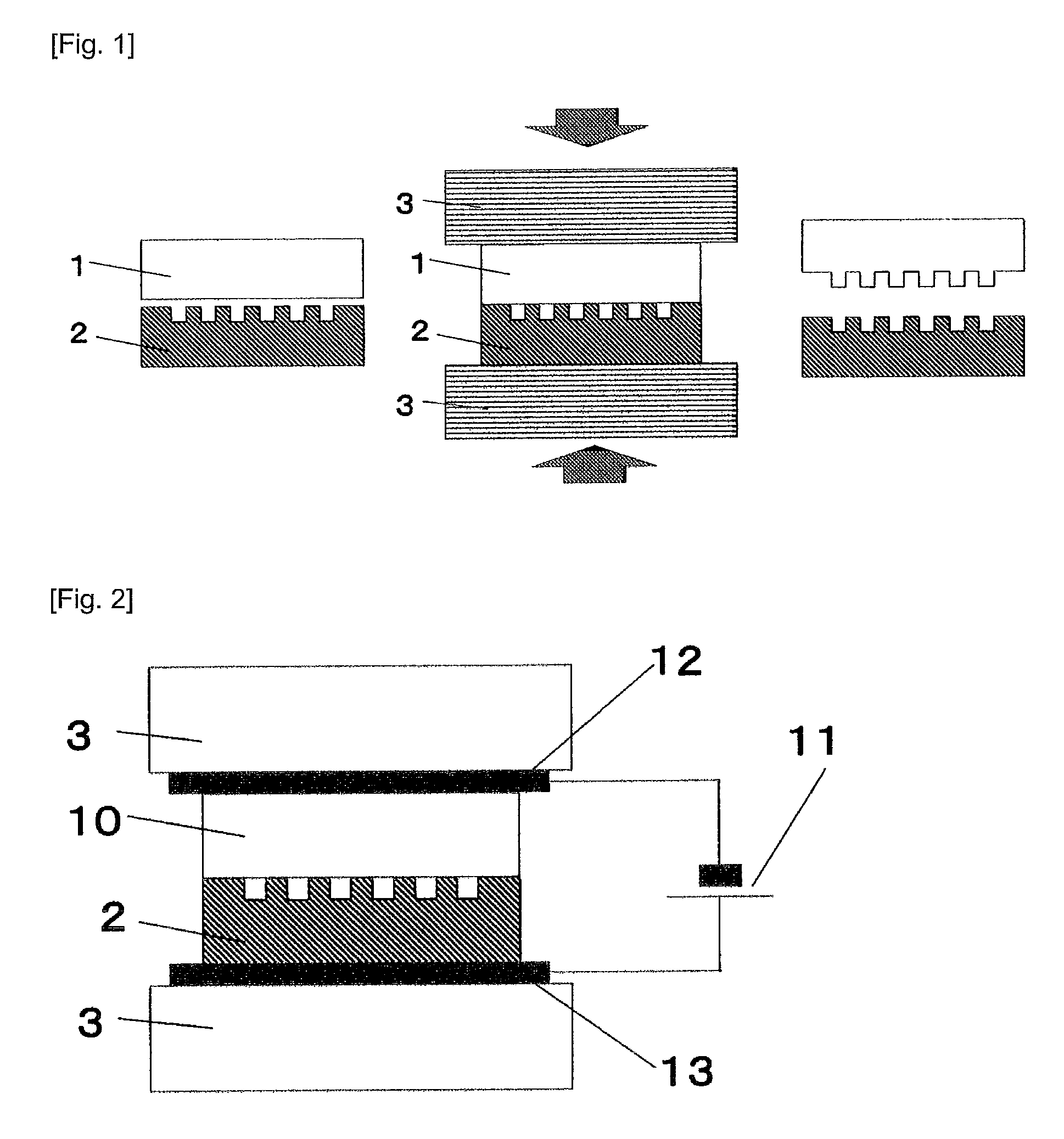
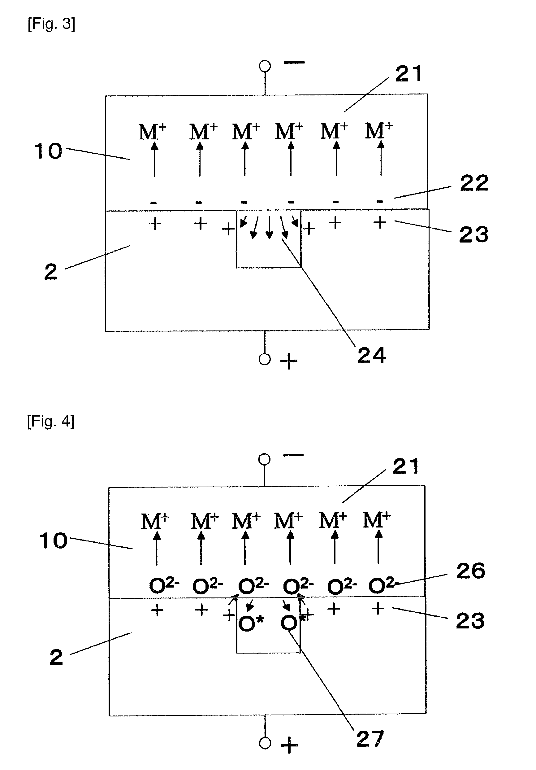
[0134]For the molding, crown glass containing potassium (0200 glass produced by MATSUNAMI GLASS IND., LTD.) was used as the glass material, and a quartz substrate having a fine line-and-space pattern formed thereon was used as the molding die. On the surface of the die, a platinum layer having a thickness of 20 nm was formed. A glass transition temperature of the crown glass was 533° C. The above-mentioned components were placed in the molding apparatus having the configuration illustrated in FIG. 7. Then, the chamber was evacuated to a vacuum. Subsequently, the glass material and the molding die were heated to 440° C. while being kept in contact with each other. A voltage at 1 kV was applied in the state that the glass side was the negative electrode and the molding die side was the positive electrode to be kept for ten minutes. No load was applied at the time of molding. It was confirmed that a profile of the die was replicated to the surface of the glass after the molding, as ill...

example 2

[0135]With use of the crown glass and the molding die made of quartz, on which the platinum film was formed, the molding was performed by applying the voltage at the time of molding, while the applied pressure at 0.5 MPa was applied for ten minutes. The conditions other than the application of the pressure were the same as those of Example 1. As a result of the application of the pressure, molding ability was improved. As the deformation of the glass material, 0.2 μm was obtained.

example 3

[0142]The molding was performed at 440° C. and 500° C. using pyrex glass (pyrex: registered trademark) manufactured by Asahi Techno Glass Co., Ltd. as the glass material. The conditions other than the temperatures at the time of molding were the same as those of Example 1. Though the deformation was about 0.01 μm at 440° C., the deformation of 0.2 μm was obtained by the molding at 500° C. Though the pyrex glass having a high softening temperature requires a high temperature for the molding, the effects of the application of the voltage are the same as those of Example 1.


PUM

PropertyMeasurementUnit
applied voltageaaaaaaaaaa
pressureaaaaaaaaaa

Abstract

A molding apparatus of a glass material according to the present invention is characterized by containing means for holding a glass material and a molding die in contact with each other, means for heating the glass material and the molding die, and means for applying a voltage across the glass material and the molding die, in which press-molding is performed by electrostatic attraction acting between a surface of the glass material and a surface of the molding die. Further, a molded product of a glass material according to the present invention is characterized by including an alkali metal as a component, in which a concentration of the alkali metal is lowered in vicinity of a surface to be molded as compared with that of a glass base material.

Description

TECHNICAL FIELD[0001]The present invention relates to mold processing of a glass material. The present invention, for example, relates to a technology for forming a micropattern on a surface of glass. In particular, the present invention is used for fabrication of an optical element used for various optical components or display devices, an optical control device employing a MEMS (Micro Electro Mechanical System), a biochemical analysis device called μ-TAS, a micro-total analysis device, a micro-chemical synthesis device, and the like.BACKGROUND ART[0002]In display devices such as flat panel displays or projectors, which have been significantly expanded in recent years, an optical element containing a large number of microstructures having a lens function or a light-scattering function is provided in front and in rear of each pixel to transmit a larger amount of light to realize a brighter image. In micro-total analysis devices, chemical synthesis devices, and fluid-controlling syst...

Claims


Application Information

Patent Timeline
Patent Type & Authority Patents(United States)
IPC IPC(8): C03B11/00B29D11/00
CPCC03B11/082C03C23/008C03B2215/07Y10T428/265C03B2215/17C03B2215/10Y02P40/57C03B11/00C03B19/00
Inventor TAKAGI, HIDEKITAKAHASHI, MASAHARUMAEDA, RYUTAROMIYAZAWA, SHINICHI
Owner NAT INST OF ADVANCED IND SCI & TECH
Learn More