Bonded intermediate substrate and method of making same

a technology of intermediate substrates and substrates, which is applied in the field of intermediate substrates, can solve the problems of reducing the usable area of light-emission, difficult and costly production of nitride semiconductors as bulk single crystals, and reducing the functionality of nitride semiconductor structures on sapphir

Active Publication Date: 2012-01-24
KONINK PHILIPS ELECTRONICS NV
View PDF75 Cites 30 Cited by
  • Summary
  • Abstract
  • Description
  • Claims
  • Application Information

AI Technical Summary

Problems solved by technology

However, nitride semiconductors are difficult and costly to produce as bulk single crystals.
Because sapphire has a low thermal conductivity and is electrically insulating, the functionality of nitride semiconductor structures on sapphire is limited.
This reduces the usable area of light-emission when compared to a GaN light-emitting device formed on conductive (i.e., highly doped semiconductor) substrates that require only one contact on the top surface and another contact on the substrate (i.e., a vertical type device).
Because both contacts are located on the top surface in a lateral device, significant lateral current flows through the chip resulting in heating of the light-emitting device which accelerates the degradation of the device.
However, these approaches present many problems, including high capital costs, resultant damage to the device layer, and low yields.
The coefficient of thermal expansion of sapphire is also poorly matched to gallium nitride and its alloys.
As a result, the growth of gallium nitride-based films on sapphire substrates presents challenges that scale with wafer diameter.
Because of these challenges, manufacturers have found it difficult to move to larger substrate sizes despite the potential for associated cost reductions.
The CTE related challenges are not addressed by post-device growth sapphire substrate removal techniques.
bstrate. At present, thinning of freestanding GaN substrates in the finished device structure is not viable due to the very high cost of the freestanding GaN substrate and the difficulty of controllably and selectively removing the thick (typically >200 μm thick) GaN substrate without damaging the thin device structure (typically <5 μ

Method used


Image

  • Bonded intermediate substrate and method of making same
  • Bonded intermediate substrate and method of making same
  • Bonded intermediate substrate and method of making same

Examples


first embodiment

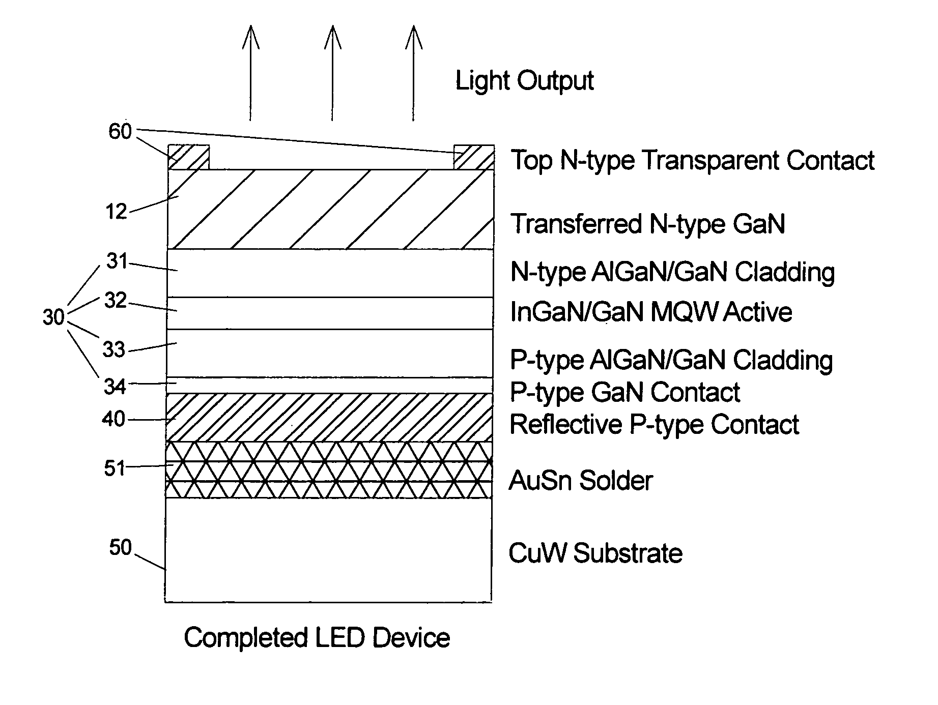
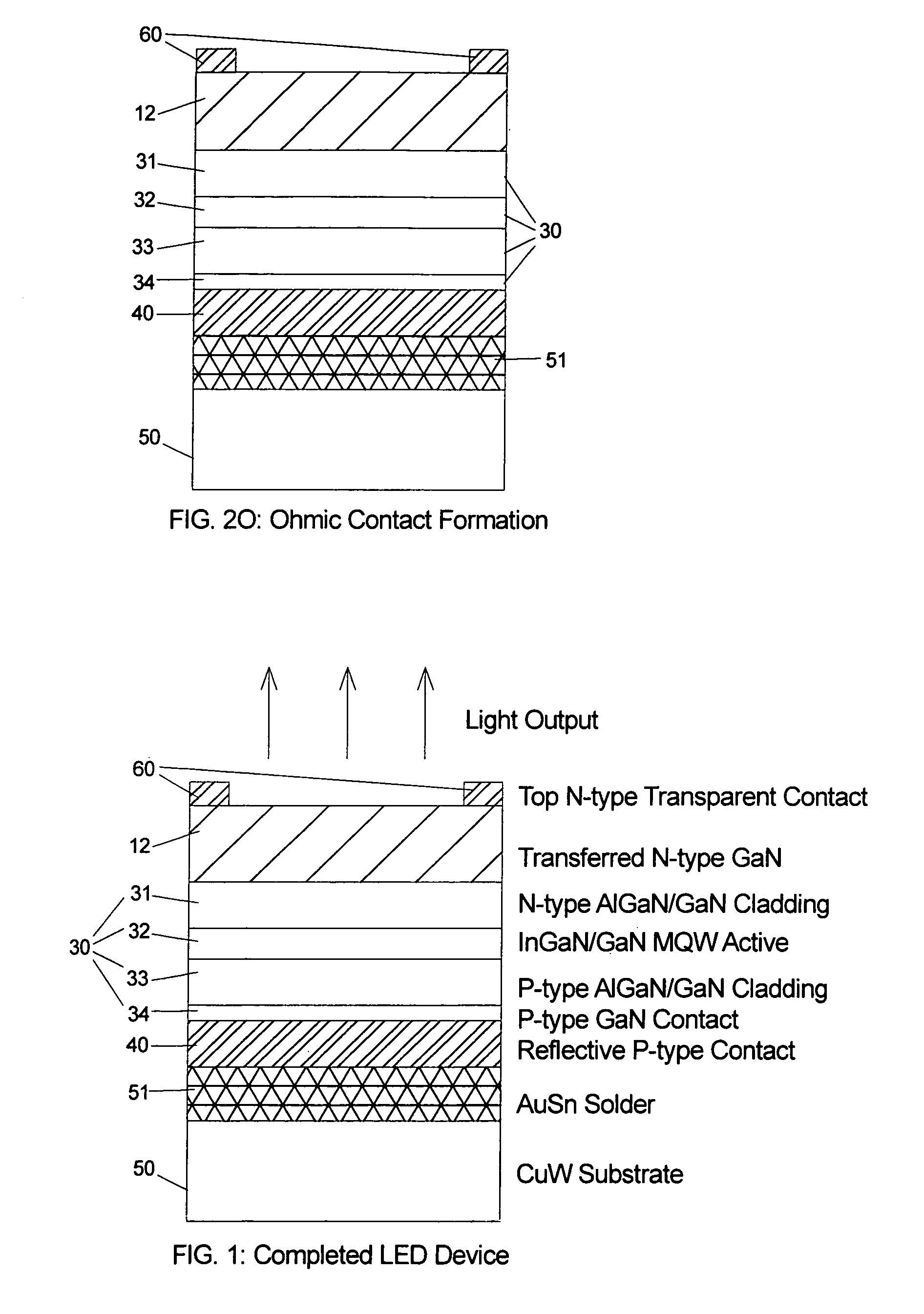
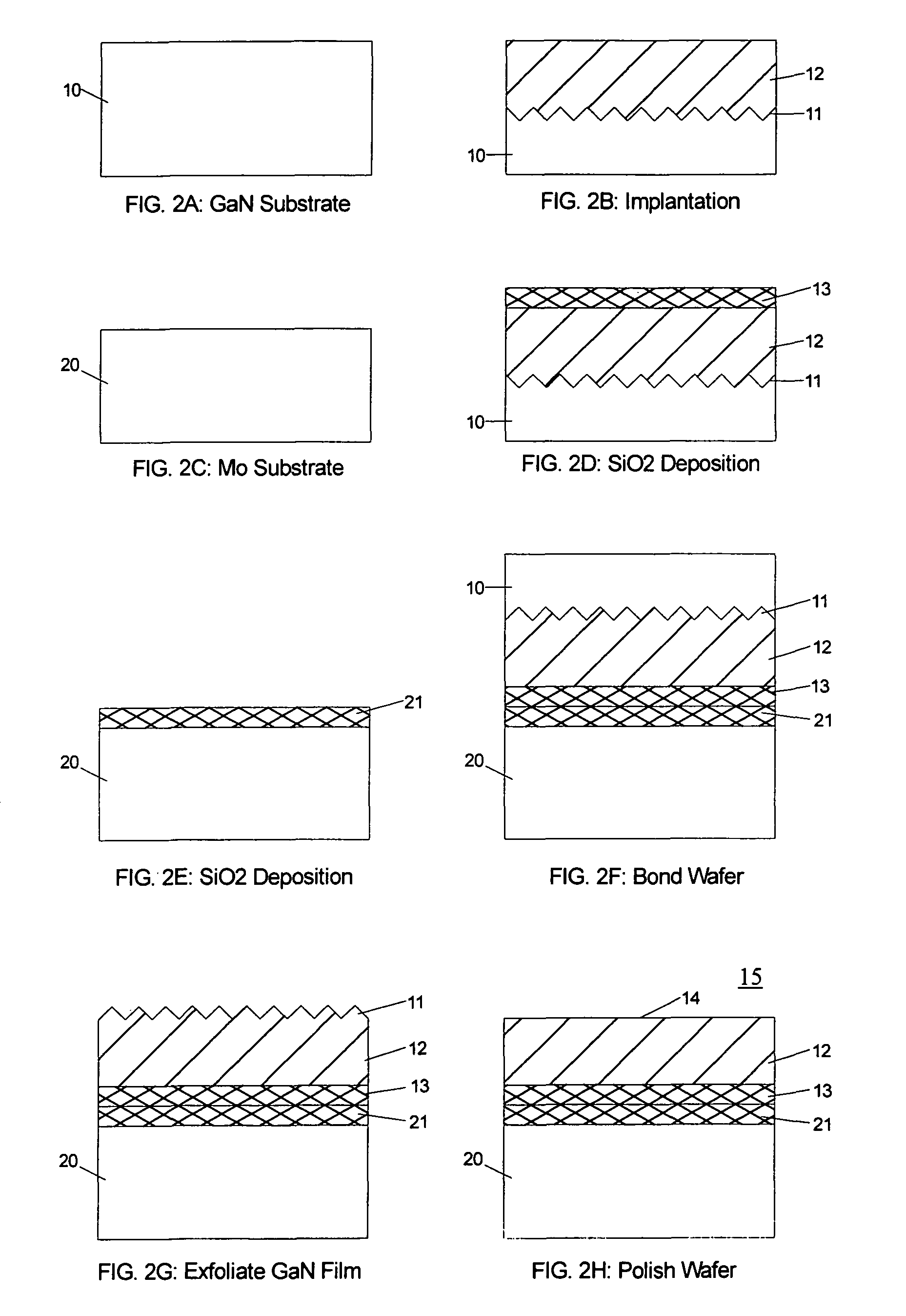
[0026]Detailed processing techniques and structures in accordance with embodiments of the present invention are illustrated in FIGS. 2A-2O, 3A-3C, 5A, and 5B. FIGS. 2A-2O illustrate a method of the In FIG. 2A, a source (also known as “donor”) semiconductor substrate or wafer 10 is preferably high-quality low-defect-density freestanding commercial GaN substrate, where dislocation-defect density is less than 108 / cm2. Other preferred candidates for source wafer 10 comprise one or more layers of GaN or AlzGa1-zN materials grown homo-epitaxially on high-quality low-defect-density freestanding commercial GaN or AlN substrates, where z is in the range of 0 to 1. Other possible candidates for source wafer 10 comprise one or more layers of GaN or AlzGa1-zN materials grown heteroepitaxially on sapphire or SiC substrates. These hetero-epitaxially grown materials have higher dislocation-defect density, typically higher than 108 / cm2.

[0027]Alternatively, as will be described with respect to the ...

second embodiment

[0161]In an alternative second embodiment, rather than bonding a III-nitride semiconductor source wafer 10 to the handle substrate and then exfoliating a thin III-nitride semiconductor layer 12 from the semiconductor source wafer, a single-crystalline material which supports epitaxial growth of III-nitride semiconductor layers is bonded to the handle substrate. This single-crystal material comprises sapphire, silicon carbide or any other suitable material which supports epitaxial growth of III-nitride semiconductor layers such as GaN, InGaN, AlGaN, etc. Thus, the GaN substrate 10 shown in FIG. 2A is substituted with a single-crystalline material comprising sapphire, SiC, or other ceramic materials.

[0162]A thin transferred layer 12 from a single-crystal material such as sapphire, may be formed on the handle substrate using an ion implantation-induced exfoliation from a bulk substrate, as shown in FIGS. 2A-2H, or using a substrate bond and etch-back process (i.e., etching and / or polis...

third embodiment

[0168]In a third embodiment, an epitaxially-grown layer on a source wafer 10 can be bonded to the handle substrate 20. Preferably, the epitaxially-grown layer on a source wafer 10 comprises a film of AlGaN grown epitaxially on a sapphire or SiC substrate, using techniques known in the art such as HVPE, MOCVD or MBE. In this embodiment the GaN source wafer 10 in FIG. 2A is substituted with an epitaxially-grown layer on a substrate comprising an AlxGa1-xN layer on a SiC or sapphire substrate, such that a thin layer of the AlxGa1-xN layer, where 0≦x≦1, is bonded and transferred to the handle substrate.

[0169]A thin transferred layer 12 of the epitaxially-grown AlGaN film may be formed on the handle substrate 20 using exfoliation or a substrate bond and etch-back process. Further processing of this third embodiment is similar to the process steps already shown in the Figures and described above.


PUM

PropertyMeasurementUnit
thicknessaaaaaaaaaa
thickaaaaaaaaaa
thickaaaaaaaaaa

Abstract

An intermediate substrate includes a handle substrate bonded to a thin layer suitable for epitaxial growth of a compound semiconductor layer, such as a III-nitride semiconductor layer. The handle substrate may be a metal or metal alloy substrate, such as a molybdenum or molybdenum alloy substrate, while the thin layer may be a sapphire layer. A method of making the intermediate substrate includes forming a weak interface in the source substrate, bonding the source substrate to the handle substrate, and exfoliating the thin layer from the source substrate such that the thin layer remains bonded to the handle substrate.

Description

CROSS-REFERENCE TO RELATED PATENT APPLICATIONS[0001]The present application claims benefit of priority of U.S. provisional application Ser. Nos. 60 / 673,367 filed on Apr. 21, 2005; 60 / 682,823 filed on May 20, 2005; 60 / 700,357 filed on Jul. 19, 2005; 60 / 703,889 filed on Aug. 1, 2005; 60 / 711,416 filed on Aug. 26, 2005; 60 / 751,308 filed on Dec. 19, 2005 and 60 / 762,490 filed on Jan. 27, 2006, all of which are incorporated herein by reference in their entirety.FIELD OF THE INVENTION[0002]The invention relates to an intermediate substrate which can be used for fabrication of wafer-bonded semiconductor structures used for light-emitting devices, such as light emitting diodes (LEDs), laser diodes (LDs), as well as other devices, and the structure of such devices. The invention further relates to wafer-bonded semiconductor structures fabricated with removable substrates.BACKGROUND OF THE INVENTION[0003]The nitride semiconductor system that includes AlxInyGa1-x-yN is a desirable direct-bandgap...

Claims


Application Information

Patent Timeline
Patent Type & Authority Patents(United States)
IPC IPC(8): H01L21/30H01L21/46H01L33/00H01L33/14H01L33/32H01L33/40
CPCB82Y20/00H01L21/2007H01L33/0079H01L33/145H01L33/32H01L2924/0002H01L33/405H01L2924/00H01L33/0093
Inventor PINNINGTON, THOMAS HENRYZAHLER, JAMES M.PARK, YOUNG-BAETSAI, CHARLESLADOUS, CORINNEATWATER, JR., HARRY A.OLSON, SEAN
Owner KONINK PHILIPS ELECTRONICS NV
Why Eureka
Try Eureka