Plasma etching device

a technology of etching device and plasma, which is applied in the direction of coating, chemical vapor deposition coating, electric discharge tube, etc., can solve the problems of difficult plasma generation on the base with high precision, and inability to achieve plasma performan

Inactive Publication Date: 2012-02-14
OHMI TADAHIRO +1
View PDF46 Cites 152 Cited by
  • Summary
  • Abstract
  • Description
  • Claims
  • Application Information

AI Technical Summary

Benefits of technology

[0006]A first plasma etching device of the present invention is provided with two parallel plate type electrodes electrode I and electrode II, and means for applying high frequency power connected to the electrode I and electrode II, with a base to be subject to etching processing using plasma being mounted on a surface of the electrode I opposite to the electrode II, and further provided with means for applying a magnetic field being horizontal with respect to the surface of the base to be subjected to plasma etching, and being unidirectional. The plasma etching device further comprises an auxiliary electrode at least on an upstream side, with respect to the base, of a flow of electrons generated by the magnetic field applying means, and the auxiliary electrode includes a local electrode arranged on the side facing the electrode II and means for adjusting impedance provided at a part of the local electrode to be electrically connected with the electrode I.

Problems solved by technology

In the field of semiconductor manufacture, etching of an oxide film or polysilicon etc. is one of the most important steps, but with a normal parallel RIE device that was used formerly it was not possible to achieve plasma performance (for example, process pressure of less than 50 mTorr, ion saturation current of at least 1 mA / cm2 (electron density of at least 1×1010 cm−3)) required for fine pattern processing at less than 1.0 μm.
However, with a magnetron plasma etching device using the above described DRM generation of low pressure high density plasma is possible, but it is very difficult to control plasma generated on the base with high precision.
That is, by introducing a horizontal magnetic field onto the base, it is to be expected that making the plasma density uniform and making the self bias potential uniform on the base will be difficult.
However, in the method of Japanese Patent Laid-open No. Sho. 62-2 1062, there was the problem that when the process pressure etc. varied, the optimal magnetic slope also varied.
On the other hand, in the method of Japanese Patent Laid-open No, 61-208223, it was anticipated from outward appearances that plasma density would be made uniform for a base in a processing space, but a mechanism for causing rotation of the magnetic field was essential, and it was difficult to miniaturize the device.

Method used


Image

  • Plasma etching device
  • Plasma etching device
  • Plasma etching device

Examples


embodiment 1

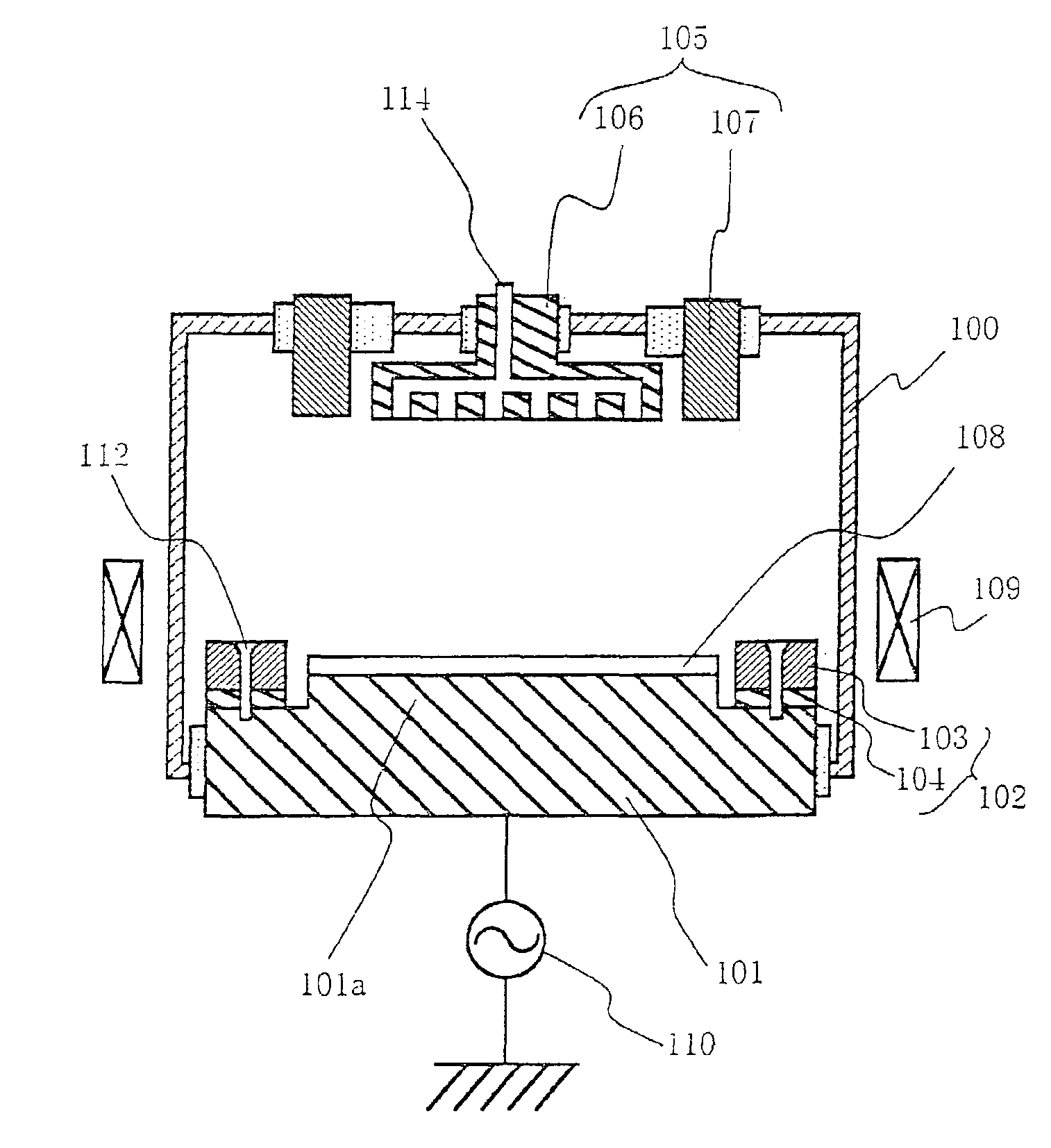
[0117]In this embodiment, a parallel plate type plasma etching device provided with the auxiliary electrode shown in FIG. 1 is used, the plasma density distribution of plasma generated when a high frequency (13.56 [MHz]) is applied to electrode I is investigated with different methods of installing the auxiliary electrode.

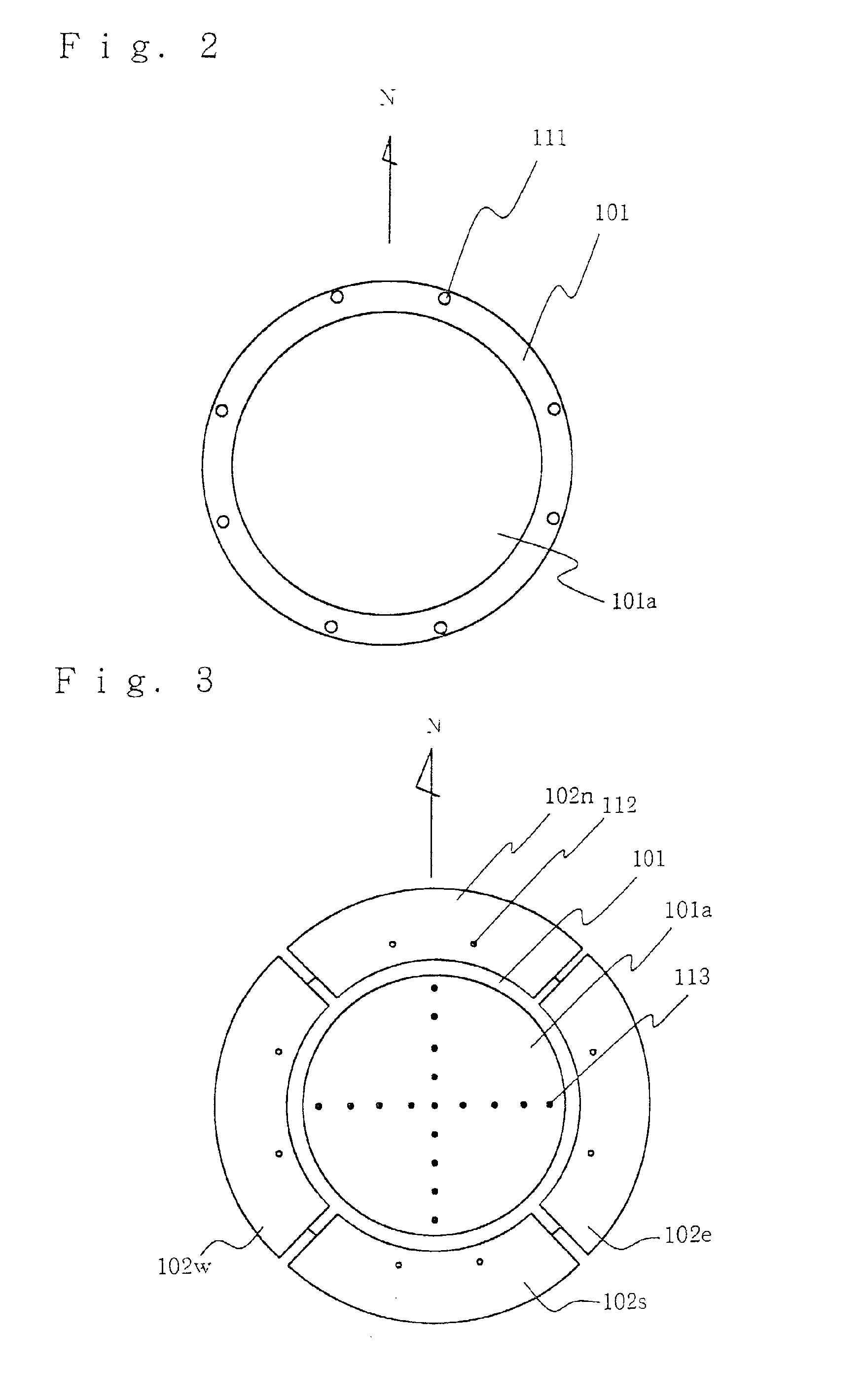
[0118]The auxiliary electrode 102 is used being divided into four parts, each part having a direction axis of one of four poles (N pole, S pole E pole and W pole) generated by the magnetic field applying means 109 as a center. The effects of the auxiliary electrode of the present invention were then investigated with one auxiliary electrode (for example, 102e) independently made a cathode (i.e. electrically short circuited to the electrode I 101) and with the remaining three auxiliary electrodes (for example, 102w, 102n and 102s) in a floating state.

[0119]The auxiliary electrode 102 comprises a local electrode 103 formed of a conductive material (Al), and junction ...

embodiment 2

[0130]This embodiment is different from embodiment 1 in that plasma density (Jion[mA / cm2])and self bias potential (Vdc[volt]) were studied using capacitors of various capacitance as the means 104e for adjusting the junction impedance of the E pole side. Cases where the capacitance of the capacitor was 1, 7, 11 and 21 [pF] and the case where the capacitor was short circuited (first embodiment) were compared.

[0131]At this time, the other three means for adjusting junction impedance (104w, 104n and 104s) were put in an electrically floating state.

[0132]The remaining points are the same as in embodiment 1.

[0133]FIG. 16 shows results of evaluating self bias potential (Vdc) for a wafer, while FIG. 17 shows results of evaluating plasma density (Jion[mA / cm2]).

[0134]From these two graphs it will be understood that that by making the junction impedance of the E pole side an optimum value (21 [pF]), Vdc higher than the case for short circuit is attained, and lowering of plasma density that wou...

embodiment 3

[0135]In this embodiment, Vdc observed when the portion of the electrode II to which high frequency power (100 [MHz]) is applied was changed was evaluated.

[0136]The remaining points were the same as for the conditions of embodiment 1 (only E pole side was made cathode).

[0137]FIG. 18 is a graph showing results for the case of application to all surfaces (106 and 107) of electrode II, FIG. 19 is a graph showing results for the case of application to only a central portion (107) of the electrode II, FIG. 2 is a graph showing results for the case of application to only an outer portion (107e) of the E pole side, and FIG. 20 is a graph showing results for the case of application to all outer electrodes (107). A schematic drawing of the electrode II is shown in the upper right corner of each drawing, and the blacked out sections of this schematic indicate portions of the electrode to which high frequency is applied.

[0138]In FIG. 18 and FIG. 19, there was no dependence on the value of appl...


PUM

PropertyMeasurementUnit
distanceaaaaaaaaaa
electron densityaaaaaaaaaa
dielectric constantaaaaaaaaaa

Abstract

A plasma etching device which has an auxiliary electrode enabling realization of a uniform plasma density of generated plasma on the surface of a base and which enables uniform etching with respect to the base without depending upon pressure and without rotating a magnetic field applying means. The plasma etching device has magnetic field applying means which has two parallel plate electrodes I and II and RF power applying means, with the base set on the electrode I, and which is horizontal and unidirectional with respect to the surface of the base where plasma etching is carried out. In this plasma etching device, an auxiliary electrode is provided at least on the upstream side of the base in a flow of electron current generated by the magnetic field applying means. The auxiliary electrode includes a local electrode arranged on the side facing the electrode II and means for adjusting impedance provided at a part of the local electrode to be electrically connected with the electrode I.

Description

CONTINUING DATA[0001]This application is a continuation of U.S. application Ser. No. 09 / 380,520 with relevant dates of Nov. 25, 1999 under 35 U.S.C. 102(e) and Nov. 26, 1999 now U.S. Pat. No. 6,585,851 date of receipt of 35 U.S.C. 371 requirements, the disclosure of which is herein explicitly incorporated by reference.TECHNICAL FIELD[0002]The present invention relates to a plasma etching device. More specifically, the present invention relates to a plasma etching device that can freely control plasma density generated on the surface of a base, and / or a self bias potential on the surface of the base.BACKGROUND OF THE INVENTION[0003]Recently, accompanying the increase in chip size of DRAM, MPU etc., there has also been a tendency to increase the diameter of a silicon substrate used as a substrate for these devices. In the field of semiconductor manufacture, etching of an oxide film or polysilicon etc. is one of the most important steps, but with a normal parallel RIE device that was u...

Claims


Application Information

Patent Timeline
Patent Type & Authority Patents(United States)
IPC IPC(8): C23F1/00C23C16/52C23C16/505H01L21/306C23C16/509C23C16/06C23C16/22H01J37/32
CPCH01J37/32082H01J37/32623H01J37/3266
Inventor OHMI, TADAHIROHIRAYAMA, MASAKITAKANO, HARUYUKIHIRAYAMA, YUSUKE
Owner OHMI TADAHIRO
Why Eureka
Try Eureka