Pattern forming method and semiconductor device manufacturing method

a semiconductor device and forming method technology, applied in semiconductor devices, basic electric elements, electrical equipment, etc., can solve problems such as difficulty in controlling the shape of patterns, increase junction leakage, and process stability, and achieve low energy consumption, high density, and refine pattern formation

Active Publication Date: 2012-02-21
NAGOYA UNIVERSITY +1
View PDF17 Cites 180 Cited by
  • Summary
  • Abstract
  • Description
  • Claims
  • Application Information

AI Technical Summary

Benefits of technology

[0006]An object of the present invention is to provide a pattern forming method and semiconductor device manufacturing method that can address miniaturization and can make plasma damage hardly caused.
[0015]Particularly, where the surface oxidation step is arranged to perform radical oxidation by use of microwave excitation plasma, the plasma that contains ions and radicals with a high density and a low energy allows the silicon oxide film to be formed with a uniform film thickness while minimizing plasma damage, suppressing the silicon plane direction dependency, and reducing the Si / SiO2 interface roughness. Accordingly, pattern formation can be performed to provide a pattern surface with high film quality and high precision by repeating formation of the silicon oxide film and removal of the silicon oxide film.

Problems solved by technology

However, where a pattern is formed by dry etching with plasma, it is difficult to control the shape of the pattern, thereby entailing a problem concerning process stability.
As regards dry etching, other problems have been found such that plasma damage, such as surface roughening, is caused to a silicon surface and / or underlying film, and that by-products generated during the etching are diffused during a thermal oxidation step subsequently performed.
The surface roughness and damaged layers thus generated may bring about problems, such as an increase in junction leakage, in semiconductor devices.
In recent years, miniaturization of semiconductor devices is making rapid progress, but photolithography techniques have come near the end of their potential concerning light exposure precision and development precision, and etching techniques have also come near the end of their potential concerning precision and shape controllability.

Method used


Image

  • Pattern forming method and semiconductor device manufacturing method
  • Pattern forming method and semiconductor device manufacturing method
  • Pattern forming method and semiconductor device manufacturing method

Examples


Embodiment Construction

[0038]An embodiment of the present invention will now be described in detail with reference to the accompanying drawings.

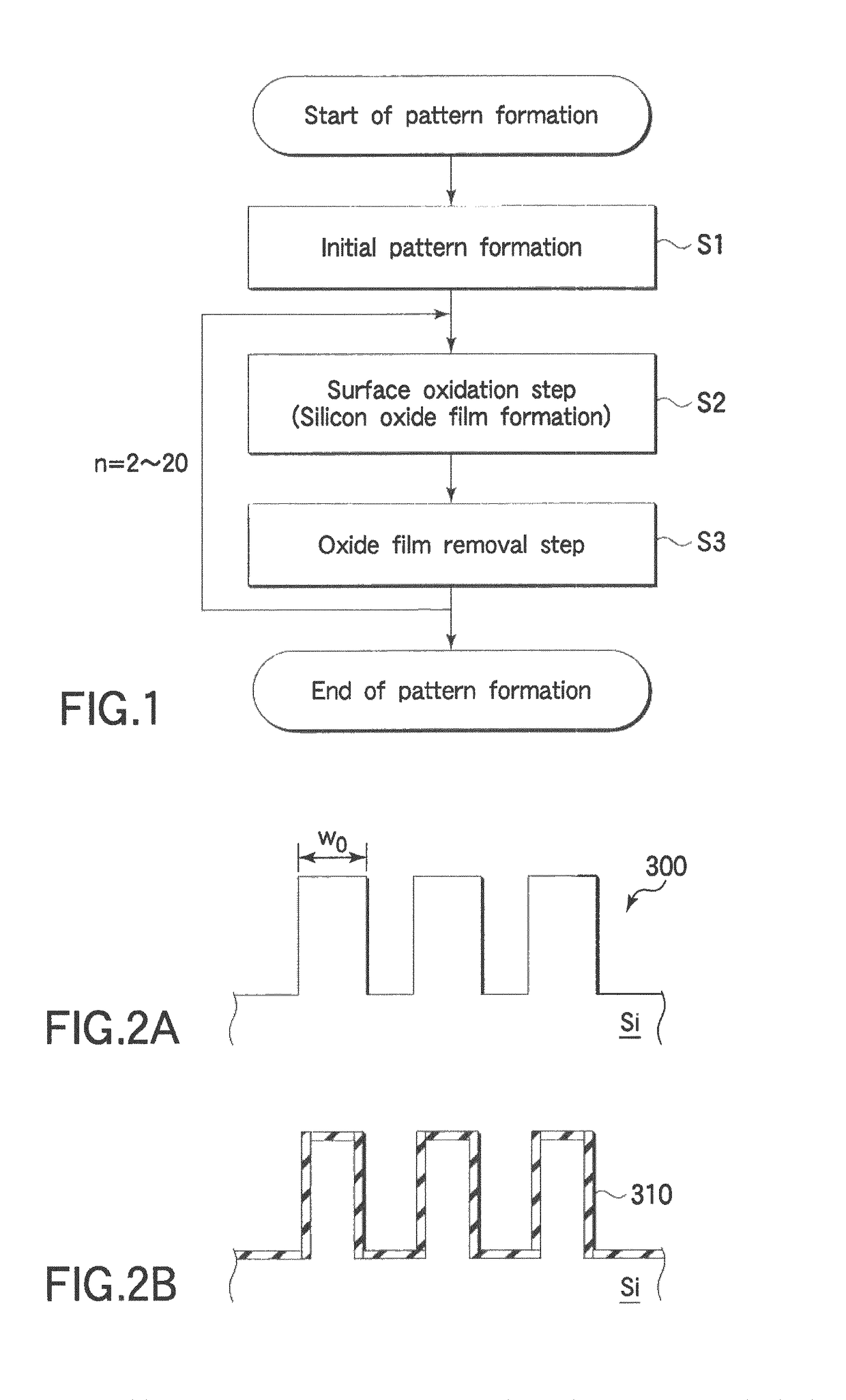
[0039]FIG. 1 is a flow chart showing a pattern forming method according to an embodiment of the present invention.

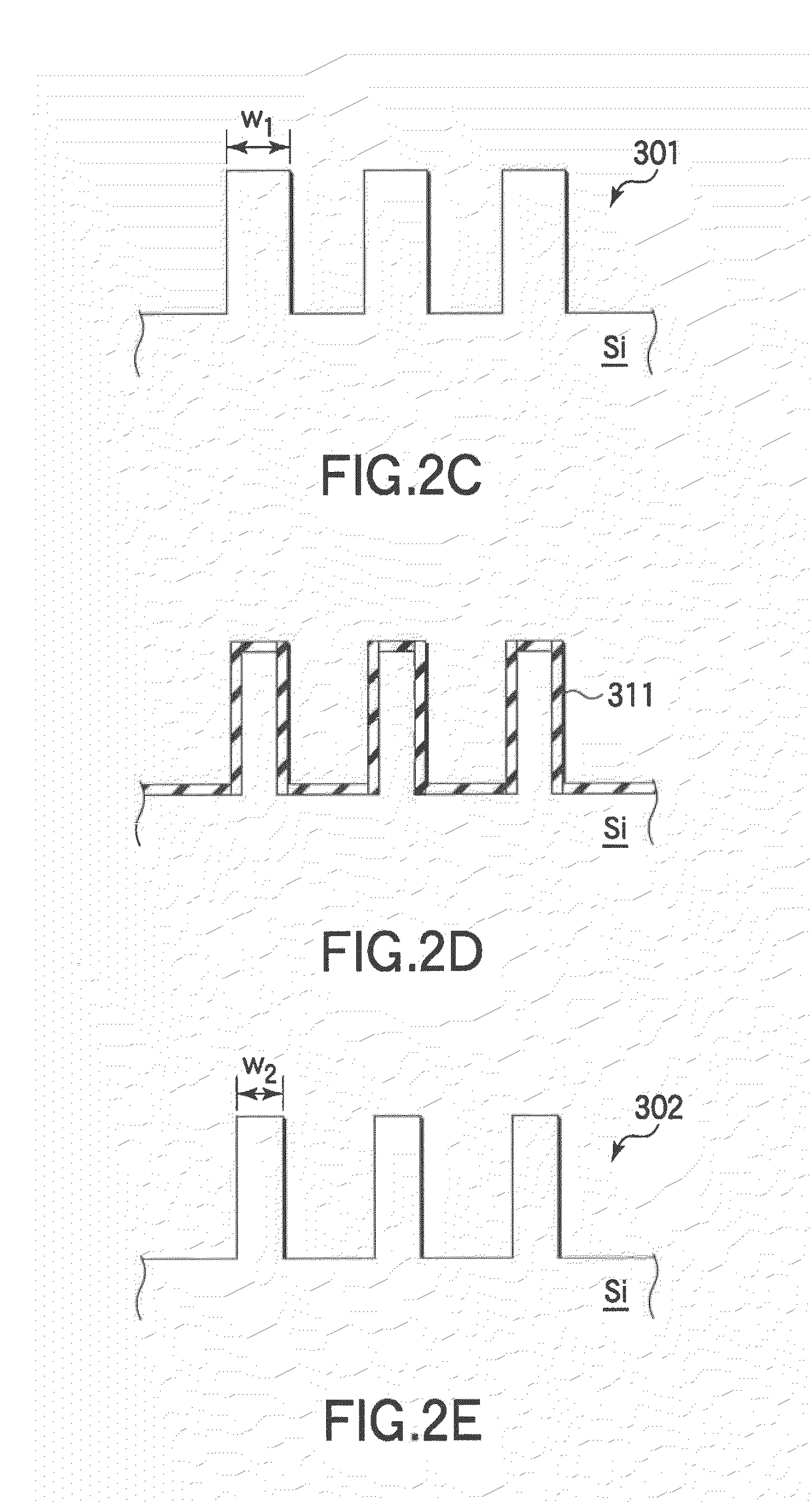
[0040]In a pattern forming method according to this embodiment, an initial pattern having a first line width is formed on a silicon surface of a target substrate (Step 1). This initial pattern may be formed by dry etching or the like through a resist mask with a pattern formed by, e.g., a photolithography technique. The surface thus etched has a surface roughness of 0.2 to 1 nm, which is acceptable, but a surface portion may be removed because part of the surface portion possibly suffers etching damage or the like.

[0041]Then, a plasma oxidation process is performed on the target substrate with the initial pattern formed thereon to oxidize the silicon surface to form a silicon oxide film (Step 2: surface oxidation step). This plasma oxidation process ma...


PUM

PropertyMeasurementUnit
widthaaaaaaaaaa
thicknessaaaaaaaaaa
pressureaaaaaaaaaa

Abstract

A pattern forming method includes preparing a target object including silicon with an initial pattern formed thereon and having a first line width; performing a plasma oxidation process on the silicon surface inside a process chamber of a plasma processing apparatus and thereby forming a silicon oxide film on a surface of the initial pattern; and removing the silicon oxide film. The pattern forming method is arranged to repeatedly perform formation of the silicon oxide film and removal of the silicon oxide film so as to form an objective pattern having a second line width finer than the first line width on the target object.

Description

TECHNICAL FIELD[0001]The present invention relates to a pattern forming method and semiconductor device manufacturing method, and specifically to a pattern forming method and semiconductor device manufacturing method that can be applied to cases where a pattern, such as a line-and-space pattern, is formed on a silicon surface in the process of manufacturing various semiconductor devices, for example.BACKGROUND ART[0002]In the process of manufacturing various semiconductor devices, a photolithography technique is used to perform patterning of a resist film formed on a target substrate surface, so as to form a resist pattern by subjecting the resist film to light exposure and development. Then, etching is performed by use of the resist pattern as a mask, thereby forming a pattern, such as a line-and-space pattern, on the target substrate. For example, there has been proposed a method that is used in the process of manufacturing a poly-crystalline silicon gate electrode, such that a re...

Claims


Application Information

Patent Timeline
Patent Type & Authority Patents(United States)
IPC IPC(8): H01L21/302H01L21/461
CPCH01L21/02238H01L21/02252H01L21/30604H01L21/31111H01L21/31116H01L21/31662H01L21/3065H01L29/66818
Inventor HORI, MASARUKABE, YOSHIROSHIOZAWA, TOSHIHIKOKITAGAWA, JUNICHI
Owner NAGOYA UNIVERSITY
Why Eureka
Try Eureka