

Reduced stiction and mechanical memory in MEMS devices
a technology of mechanical memory and d-x bonds, which is applied in the direction of semiconductor devices, semiconductor/solid-state device details, electrical apparatus, etc., can solve the problem of reducing the bonding vibrational constant for d-, and achieve the effect of reducing the isomerization, exchange and atom transfer rate of surface reactions, and reducing the static friction between the contact surfaces of mems components
- Summary
- Abstract
- Description
- Claims
- Application Information
AI Technical Summary
Benefits of technology
Problems solved by technology
Method used
Image

Examples
first embodiment
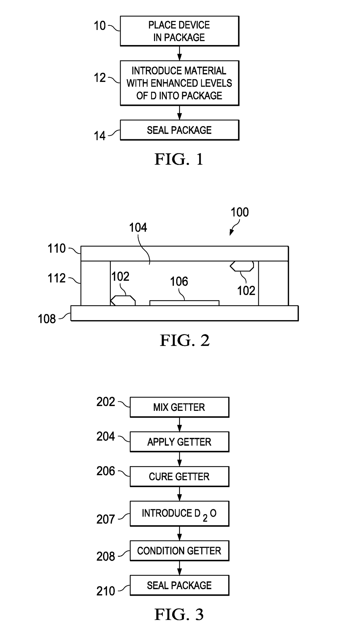
[0024]In the present invention, water vapor (H2O) normally present in a packaged MEMS device is replaced with heavy water vapor (D2O) in the packaging process.
[0025]FIG. 2 illustrates a cross-section of a microelectromechanical device package 100. A getter, or desiccant, compound 102 performs a desiccation function as well as providing a reversible source / sink of passivation material in a headspace 104 in which a micromechanical device 106 is enclosed. While the following description describes its use with a PFDA surface treatment material and micromirror device, these examples are for illustration purposes and in no way limit the intended scope of the disclosed invention. The disclosed technology is ideal for any micromechanical device used with an acidic passivant. A preferred embodiment of the passivant is described in U.S. Pub. No. 2008 / 016,268, which is incorporated by reference herein.
[0026]The disclosed desiccant compound has two primary components, a polymer and a drying age...
second embodiment
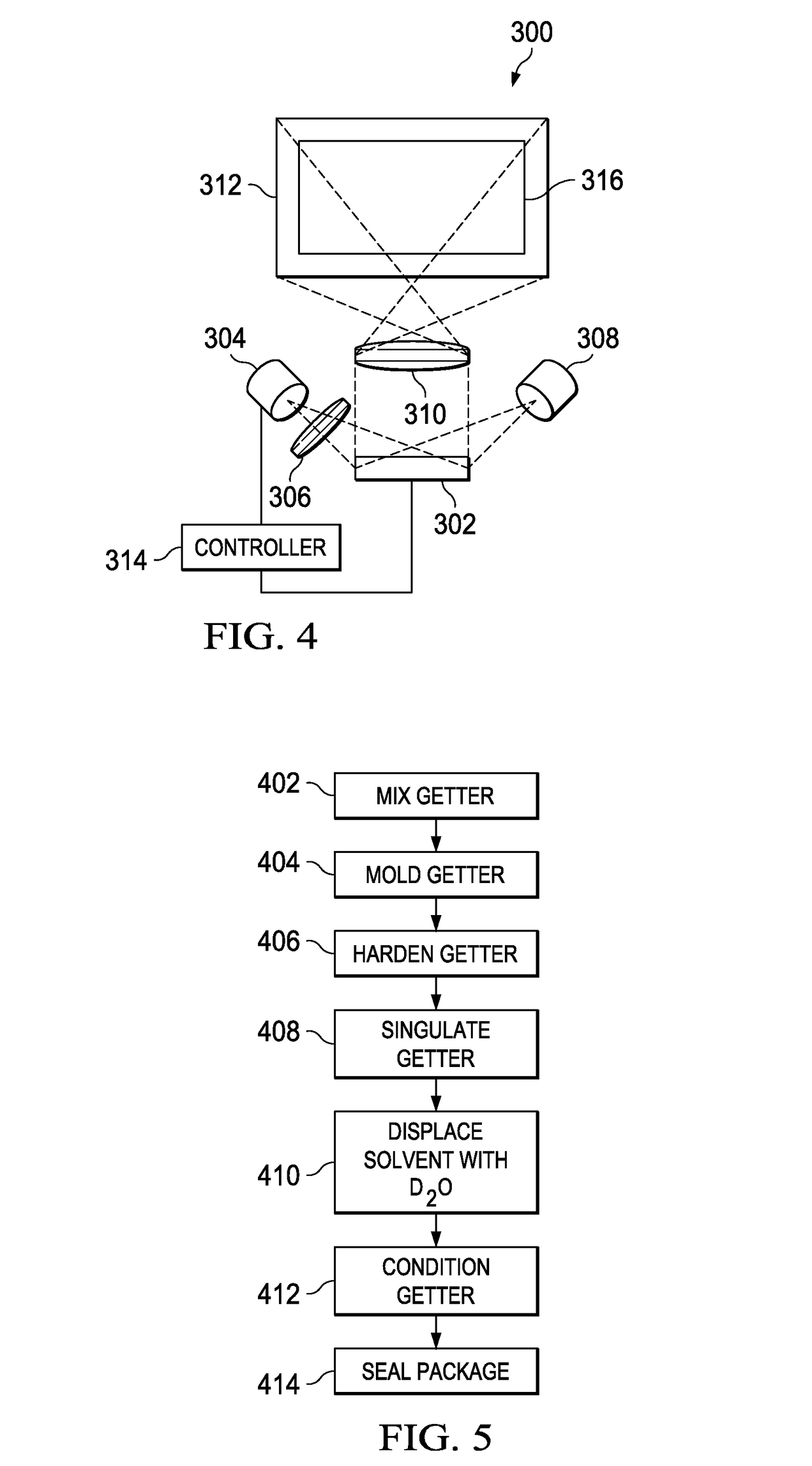
[0040]FIG. 5 illustrate replacing H with D inside the package. In FIG. 5, the getter for the MEMs device is prepared by mixing a zeolite and an organic binder in a solvent to form a paste in step 402. Hexanol is a typical solvent. The paste is then cast or molded into the desired shape in step 404. In step 406, the solvent evaporates quickly from the paste, allowing the binder to harden. Getters are often formed in sheets and cut into individual pieces, called dibs, after the sheets have hardened as indicated by step 408. The individual pieces, however, can be separated at virtually any step of the process. Even after the binder is dried, significant amounts of solvent remain bound up by the zeolite. In the case of a micromirror device, a passivation coating, such as PFDA, is included in the sealed package to reduce the stiction forces and ensure long term operation of the device.
[0041]The solvent retained by the zeolite in the getter can have detrimental effects on the operation of...
third embodiment
[0048]the present invention is to using a passivation coating including deuterium in step 12 of FIG. 1. Exposing the surface of a MEMS device using a carboxylic acid passivation coating, such PFDA is described in U.S. Pat. Nos. 5,331,454 and 5,602,671.
[0049]In general, a small quantity of the passivating source material is placed in a container with the MEMS device in a vacuum oven. As the passivating source material melts, it produces a vapor that deposits a passivating layer on the exposed and activated surfaces of the devices. After the deposition is finished, the cover of the container is removed and the oven is evacuated and continuously pumped to eliminate any excess source material, ensuring that only the passivating layer remains on the devices.
[0050]In this embodiment of the invention, rather than use a carboxylic acid of the type R—COOH, where R═CH3(CH2)n, as the source material, a variation using deuterium is used in its place. For example, a source material of CD3(CD2)nC...
PUM
 Abstract
Description
Claims
Application Information