Method and structure for thick layer transfer using a linear accelerator

a linear accelerator and thick layer technology, applied in accelerators, electrical devices, semiconductor devices, etc., can solve the problems of insufficient optimum properties of solar cells, many limitations of solar cells, and difficult manufacturing of materials, so as to reduce the amount of semiconductor materials, enhance the stress in the cleave region, and achieve high energy implantation.

Inactive Publication Date: 2012-02-28
SILICON GENERAL CORPORATION
View PDF70 Cites 27 Cited by
  • Summary
  • Abstract
  • Description
  • Claims
  • Application Information

AI Technical Summary

Benefits of technology

[0015]In a specific embodiment, the present invention provides a method for fabricating free standing thickness of materials using one or more semiconductor substrates, e.g., single crystal silicon, polycrystalline silicon, polysilicon, silicon germanium, germanium, group III / IV materials, and others. In a specific embodiment, the present method includes providing a semiconductor substrate having a surface region and a thickness. The method includes subjecting the surface region of the semiconductor substrate to a first plurality of high energy particles generated using a linear accelerator to form a region of a plurality of gettering sites within a cleave region, the cleave region being provided beneath the surface region to defined a thickness of material to be detached, the semiconductor substrate being maintained at a first temperature. In a specific embodiment, the method includes subjecting the surface region of the semiconductor substrate to a second plurality of high energy particles generated using the linear accelerator, the second plurality of high energy particles being provided to increase a stress level of the cleave region from a first stress level to a second stress level. In a preferred embodiment, the semiconductor substrate is maintained at a second temperature, which is higher than the first temperature. The method frees the thickness of detachable material using a cleaving process, e.g., controlled cleaving process.
[0018]According to embodiments of the present invention, a free standing film may be separated from a bulk material. In one embodiment, a free standing layer of semiconductor material such as single crystal silicon, having a thickness of 20 m or greater, may be cleaved from a bulk ingot utilizing high energy implantation. In one embodiment, the cleaving involves implanting ions at a first, lower temperature to create a cleave region, and then implanting ions at a second, higher temperature to enhance stress in the cleave region. Cleaving the ingot in this manner substantially reduces the amount of semiconductor material that is otherwise lost to the kerf in a conventional blade cutting process. The resulting cleaved free standing film may be particularly suited for use in the collection of solar energy.

Problems solved by technology

Unfortunately, such petroleum sources have become depleted and have lead to other problems.
Although effective, these solar cells still have many limitations.
These materials are often difficult to manufacture.
Although these plates may be formed effectively in a cost effective manner, they do not possess optimum properties for highly effective solar cells.
In particular, polysilicon plates do not exhibit the highest possible efficiency in capturing solar energy and converting the captured solar energy into usable electrical power.
Such single crystal silicon is, however, expensive to manufacture and is also difficult to use for solar applications in an efficient and cost effective manner.
Generally, thin-film solar cells are less expensive by using less silicon material but their amorphous or polycrystalline structure are less efficient than the more expensive bulk silicon cells made from single-crystal silicon substrates.
Additionally, both polysilicon and single-crystal silicon materials suffer from material losses during conventional manufacturing called “kerf loss”, where the sawing process eliminates as much as 40% and even up to 60% of the starting material from a cast or grown boule and singulate the material into a wafer form factor.
This is a highly inefficient method of preparing thin polysilicon or single-crystal silicon plates for solar cell use.
However, an amount of silicon material corresponding to this saw thickness (the kerf) is lost by this cutting.
Use of even the thinnest saw blade that can reliably be used to saw the ingot, may result in losses of expensive, pure single crystal silicon to the kerf.
Use of the conventional wafer sawing technique can thus result in kerf losses of expensive, pure starting material amounting to as high as 60% of the entire ingot.
Another disadvantage of the conventional ID sawing technique is that slices can only be separated one at a time, thus limiting throughput and elevating cost.
While effective, conventional wire sawing also offers disadvantages, in particular a still significant kerf loss of about 50% attributable to the thickness of the wire, and possible contamination by exposure of the substrate to the oil and abrasives.

Method used


Image

  • Method and structure for thick layer transfer using a linear accelerator
  • Method and structure for thick layer transfer using a linear accelerator
  • Method and structure for thick layer transfer using a linear accelerator

Examples


Embodiment Construction

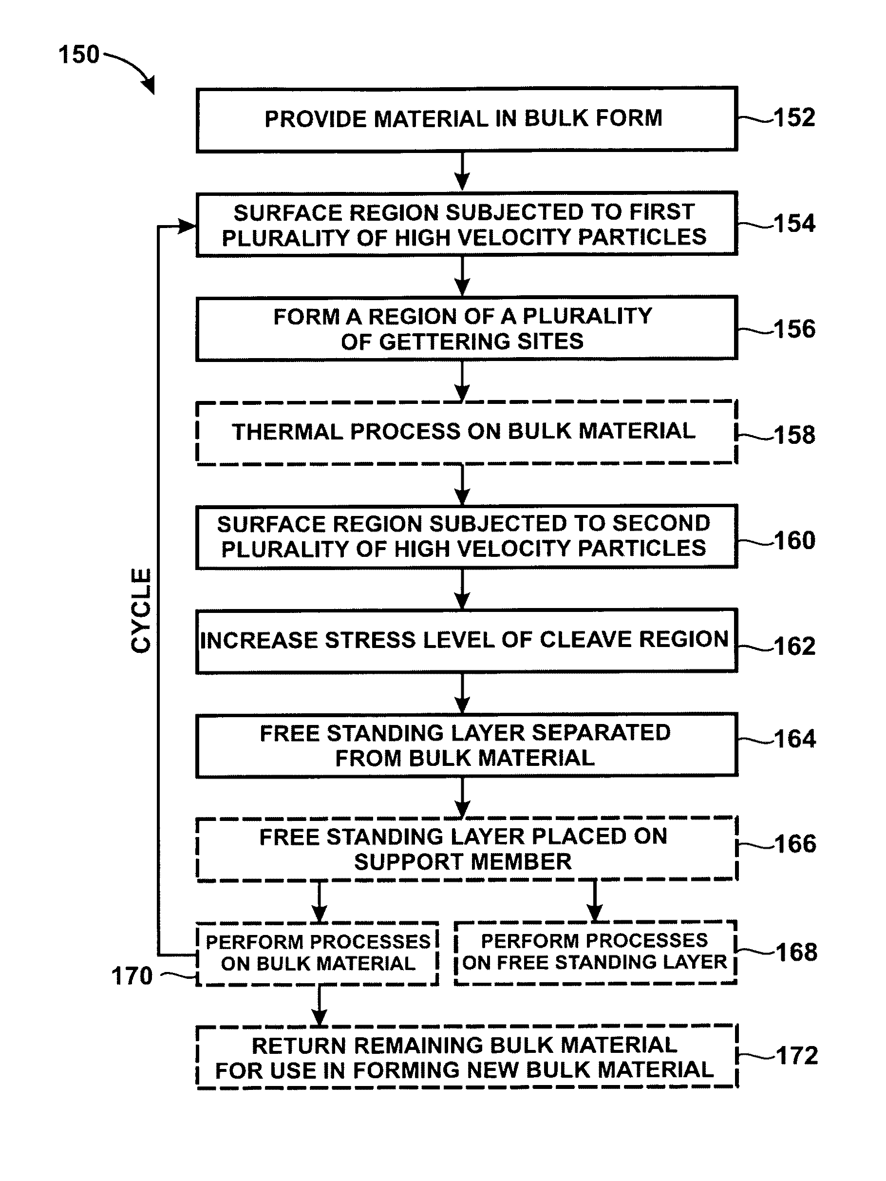
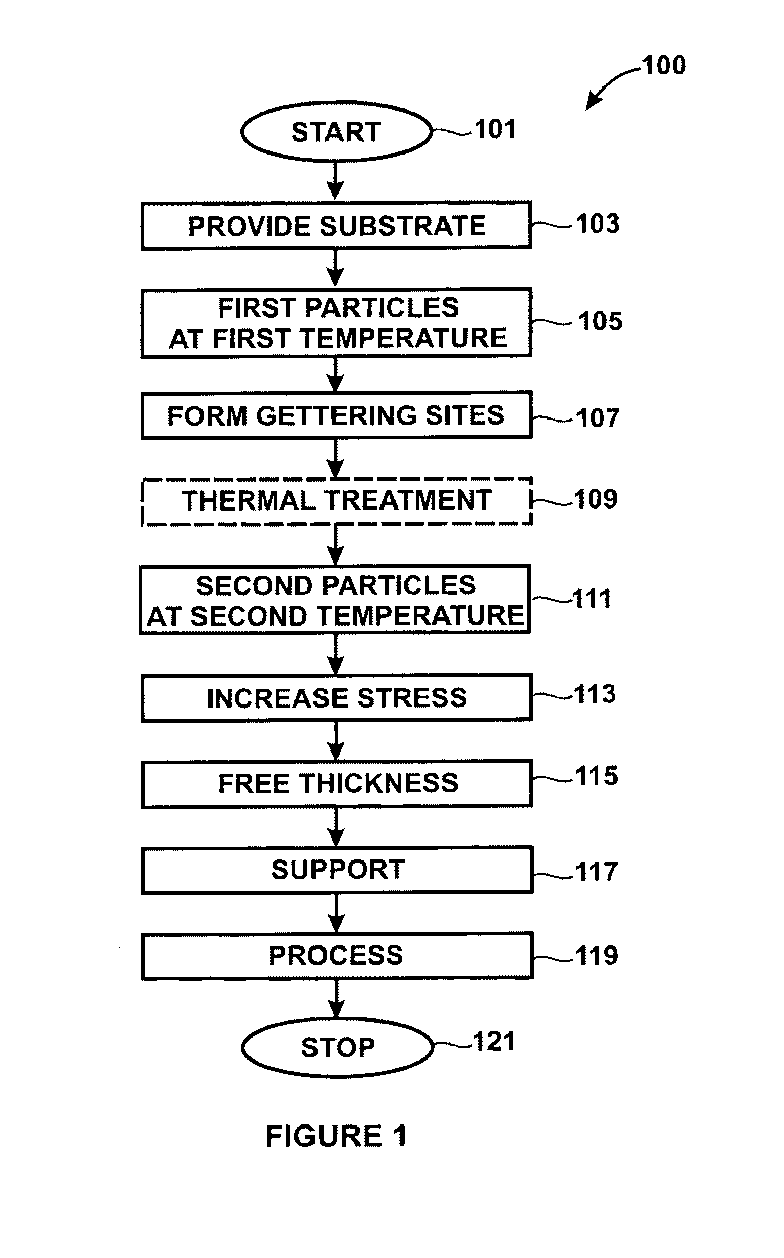
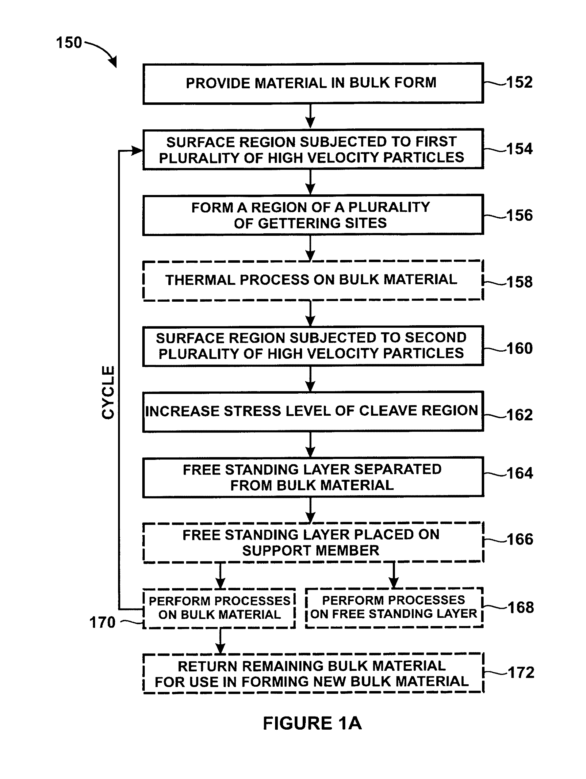
[0040]According to embodiments of the present invention, techniques including a method for forming substrates are provided. More particularly, embodiments according to the present invention provide a method to form a free standing layer of material from a semiconductor material. In a specific embodiment, the free standing layer of material is provided using a plurality of high energy particles to cause a formation of a cleave plane in the semiconductor substrate. The method according to present invent invention can be used in a variety of application, including but not limited to semiconductor device packaging, photovoltaic cells, MEMS devices, and others.

[0041]According to embodiments of the present invention, a free standing film may be separated from a bulk material. In one embodiment, a free standing layer of semiconductor material such as single crystal silicon, having a thickness of 20 μm or greater, may be cleaved from a bulk ingot utilizing high energy implantation. In one e...


PUM


Abstract

Free standing thickness of materials are fabricated using one or more semiconductor substrates, e.g., single crystal silicon, polysilicon, silicon germanium, germanium, group III / IV materials, and others. A semiconductor substrate is provided having a surface region and a thickness. The surface region of the semiconductor substrate is subjected to a first plurality of high energy particles generated using a linear accelerator to form a region of a plurality of gettering sites within a cleave region, the cleave region being provided beneath the surface region to defined a thickness of material to be detached, the semiconductor substrate being maintained at a first temperature. The surface region of the semiconductor substrate is subjected to a second plurality of high energy particles generated using the linear accelerator, the second plurality of high energy particles being provided to increase a stress level of the cleave region from a first stress level to a second stress level.

Description

CROSS-REFERENCES TO RELATED APPLICATIONS[0001]The instant nonprovisional patent application claims priority to the following provisional patent applications, each of which is incorporated herein by reference for all purposes: U.S. Provisional Patent Application No. 60 / 864,584, filed Nov. 6, 2006; and U.S. Provisional Patent Application No. 60 / 886,827, filed Jan. 26, 2007.BACKGROUND OF THE INVENTION[0002]The present invention relates generally to technique including a method and a structure for forming substrates using a layer transfer technique. More particularly, the present method and system provides a method and system using a linear accelerator process for the manufacture of thick free standing semiconductor films for a variety of applications including photovoltaic cells. But it will be recognized that the invention has a wider range of applicability; it can also be applied to other types of applications such as for three-dimensional packaging of integrated semiconductor device...

Claims


Application Information

Patent Timeline
Patent Type & Authority Patents(United States)
IPC IPC(8): H01L21/00H01L21/30H01L21/46H01L21/302H01L21/78H01L31/04H05H9/00
CPCH01L21/26506H01L21/3221H01L21/76254H01L21/2658H01L21/26593Y02E10/50H01L21/78H01L21/302H05H9/00H01L31/04
Inventor HENLEY, FRANCOIS J.LAMM, ALBERTADIBI, BABAK
Owner SILICON GENERAL CORPORATION
Why Eureka
Try Eureka