Non-volatile memory device with a silicon nitride charge holding film having an excess of silicon

a non-volatile semiconductor and charge holding film technology, applied in semiconductor devices, electrical devices, transistors, etc., can solve the problems of significant reduction of data holding characteristics, difficult increase in the number of rewriting, so as to suppress the deterioration of the subthreshold coefficient, improve the performance of the non-volatile semiconductor storage device, and improve the durability of rewriting

Active Publication Date: 2012-02-28
RENESAS ELECTRONICS CORP
View PDF14 Cites 25 Cited by
  • Summary
  • Abstract
  • Description
  • Claims
  • Application Information

AI Technical Summary

Benefits of technology

[0019]Although the electron writing using hot electrons and hole erasure using hot holes enable low-voltage and high-speed programming, it is difficult to increase the number of rewriting. This is for the reason that the hole erasure using hot holes deteriorates the film quality of the bottom Si oxide film, and the film quality deterioration leads to significant reduction in the data holding characteristic. Deterioration in the data holding characteristic include a deterioration mode in which a threshold voltage (Vth) in the writing side is reduced along with left time (deterioration is maximum at a high temperature) and a deterioration mode in which Vth in the erasure side increases (deterioration is maximum in the vicinity of room temperature), and increase in Vth the erasure side particularly makes the increase in the number of rewriting difficult. Therefore, in the MONOS memory using the hot electrons and hot holes in programming, how to reduce the injection amounts of both the electric charges so as to prevent deterioration of the film quality of the bottom Si oxide film is a key to improve rewriting durability.
[0030]As described above, since the phenomenon of the local presence of both the electric charges in terms of space and energy leads to increase in the electric charge injection amount (time) along with a rewriting operation, deterioration of the film quality of the bottom Si oxide film is accelerated. Eventually, the deterioration of the film quality of the bottom Si oxide film significantly reduces the data holding characteristic (retention characteristic); therefore, the number of rewriting of the MONOS memory is limited.
[0031]An object of the present invention is to improve performance of a non-volatile semiconductor storage device which performs electron writing by hot electrons and hole erasure by hot holes, in particular, to improve the rewriting durability by suppressing increase in injection amounts of both electric charges accompanying rewriting. Also, another object of the present invention is to improve the rewriting durability by suppressing deterioration of the subthreshold coefficient. Also, another object is to improve the data holding characteristic.
[0039]Performance of a non-volatile semiconductor storage device which performs electron writing by hot electrons and hole erasure by hot holes can be improved. Particularly, rewriting durability can be improved by suppressing increase in the both electric charge injection amount accompanying rewriting. In other words, by suppressing deterioration of the subthreshold coefficient, the rewriting durability can be improved, and the data holding characteristic can be improved.

Problems solved by technology

Although the electron writing using hot electrons and hole erasure using hot holes enable low-voltage and high-speed programming, it is difficult to increase the number of rewriting.
This is for the reason that the hole erasure using hot holes deteriorates the film quality of the bottom Si oxide film, and the film quality deterioration leads to significant reduction in the data holding characteristic.
Deterioration in the data holding characteristic include a deterioration mode in which a threshold voltage (Vth) in the writing side is reduced along with left time (deterioration is maximum at a high temperature) and a deterioration mode in which Vth in the erasure side increases (deterioration is maximum in the vicinity of room temperature), and increase in Vth the erasure side particularly makes the increase in the number of rewriting difficult.
Upon recombination of the electrons and the holes, energy corresponding to the energy difference between the trap levels is emitted, and this energy cuts the combinations in the ONO film; thus, deterioration of the film quality of the ONO film is caused.

Method used


Image

  • Non-volatile memory device with a silicon nitride charge holding film having an excess of silicon
  • Non-volatile memory device with a silicon nitride charge holding film having an excess of silicon
  • Non-volatile memory device with a silicon nitride charge holding film having an excess of silicon

Examples


first embodiment

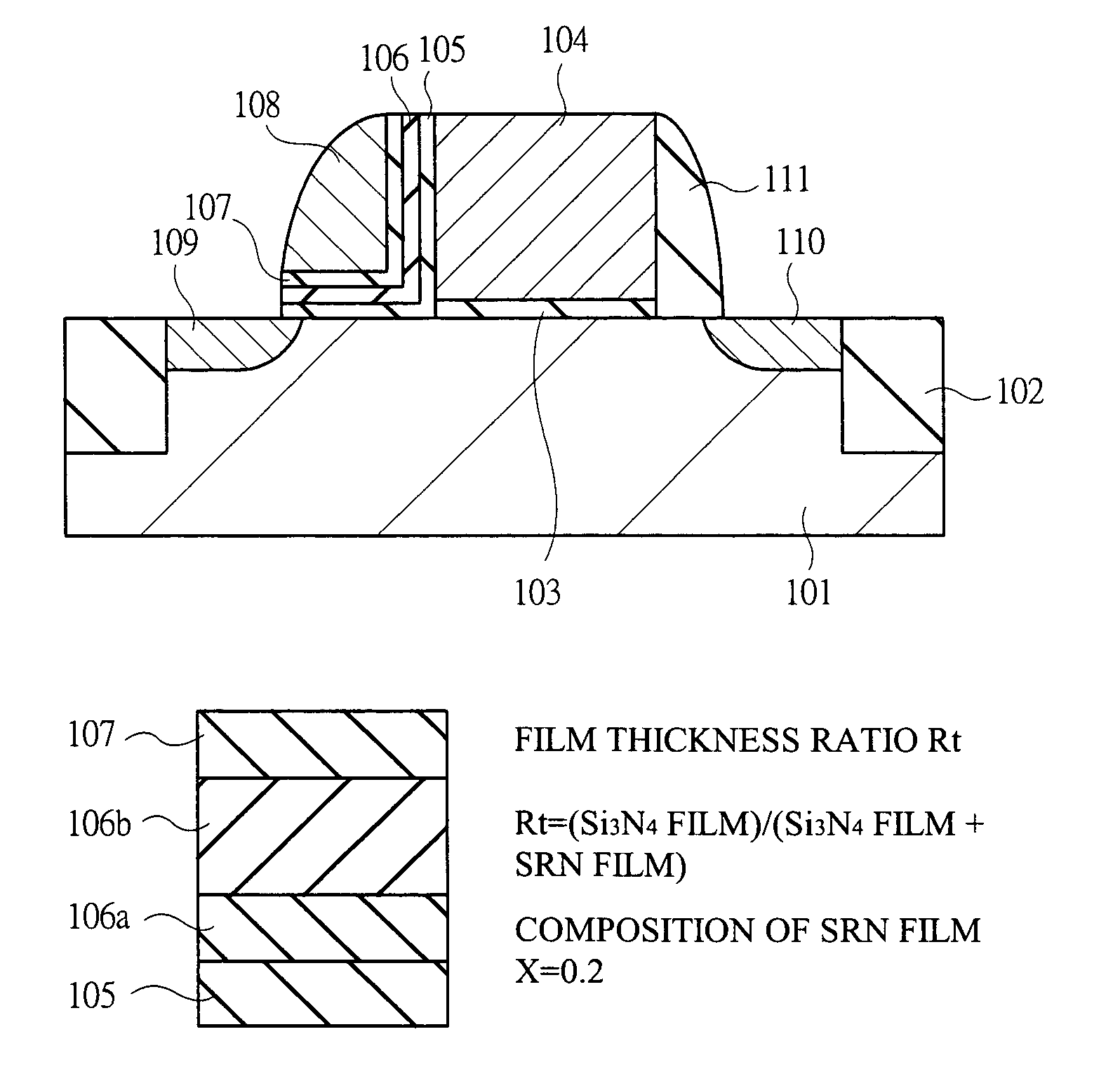
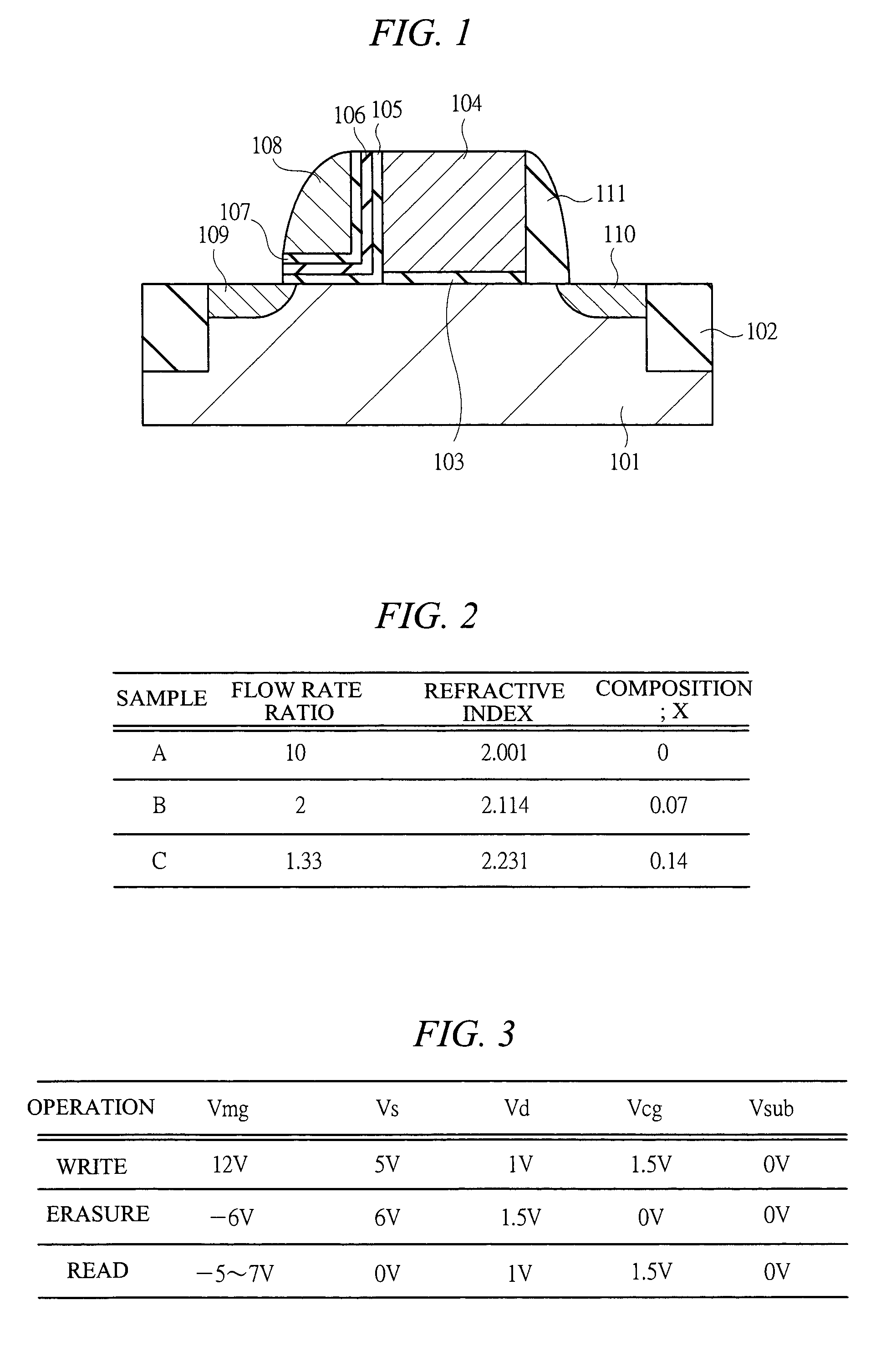
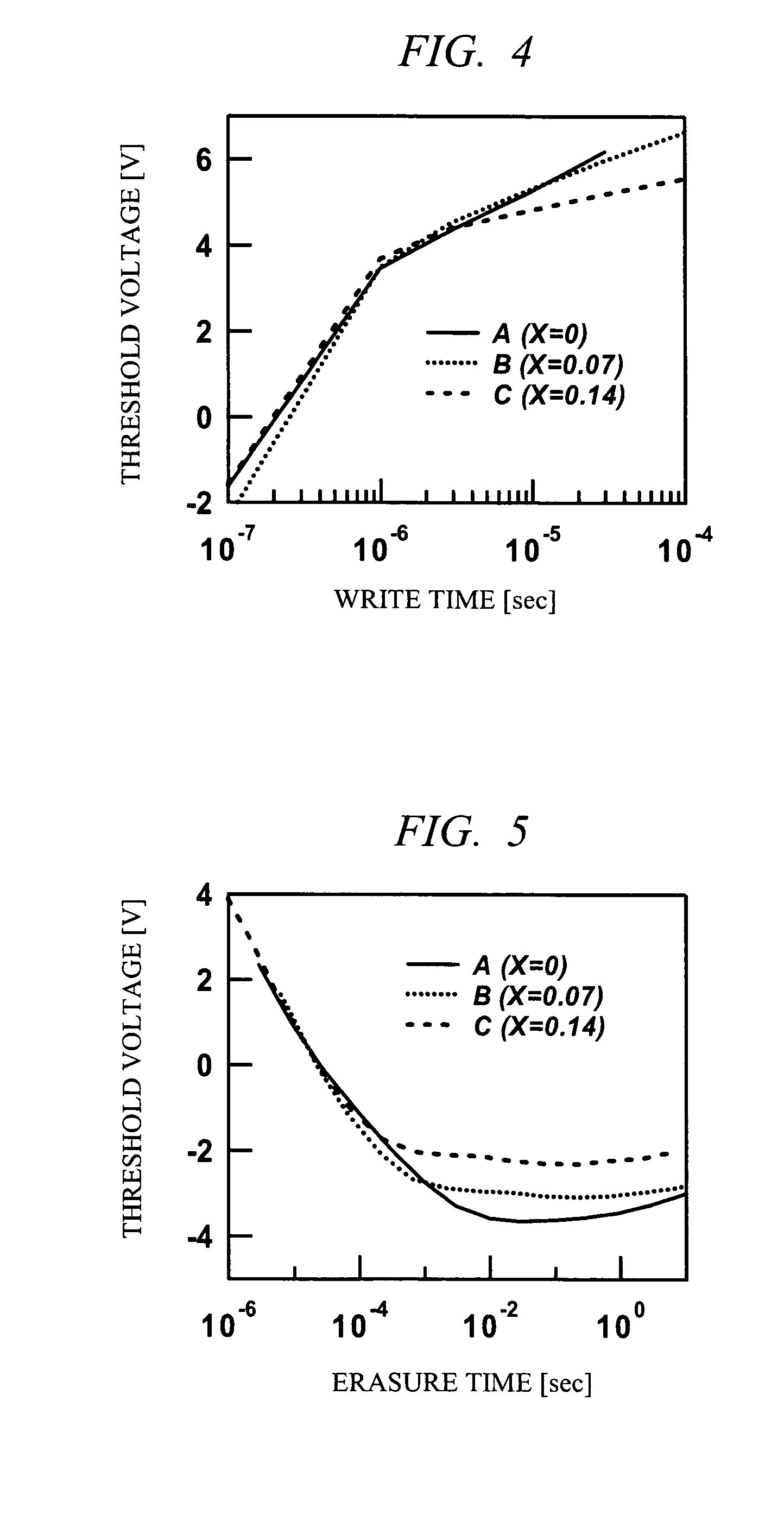
[0091]A first embodiment of the present invention will be described in detail by using FIG. 1 to FIG. 14. FIG. 1 is a diagram showing a cross sectional view of a non-volatile memory cell which is the first embodiment of the present invention. In practice, wiring is present in an upper layer of the drawing; however, it is omitted in this drawing. FIG. 2 shows samples fabricated in the first embodiment. The first embodiment provides examples in which, as shown in FIG. 2, as an electric charge holding film, a sample A using a film having a stoichiometrical ratio of Si3N4, a sample B using an SRN film into which silicon atoms (Si) are stoichiometrically excessively introduced, and a sample C using an SRN film into which silicon atoms (Si) are stoichiometrically excessively introduced are fabricated. The SRN film compositions of the sample B and the sample C are different, and the SRN film of the sample C further excessively contains Si. In the first embodiment, except for the electric h...

second embodiment

[0135]A second embodiment of the present invention will be described in detail by using FIG. 15 to FIG. 24. A non-volatile memory cell which is the second embodiment of the present invention has a structure which is basically same as the structure shown in FIG. 1 of the first embodiment, and merely the configuration of the electric charge holding film 106 and the composition of the SRN film are different.

[0136]FIG. 15 shows the configuration of a capacitance insulating film of the memory transistor of the second embodiment. In the second embodiment, the electric charge holding film is formed by a laminated structure of an SRN film 106a stoichiometrically excessively containing silicon and a stoichiometrically Si3N4 film 106b. The composition of the SRN film 106a is x=0.2, and the film thickness ratio of the SRN film 106a and the Si3N4 film 106b is used as a parameter. The composition of the SRN film used in the second embodiment is x=0.2 and excessively contains Si more than the fir...

third embodiment

[0150]Next, a third embodiment of the present invention will be described by using FIG. 25 to FIG. 27. A non-volatile memory cell which is the third embodiment of the present invention is a non-volatile memory cell composed of one memory transistor as shown in FIG. 25; however, basically, it has a structure approximately same as the structure of the memory transistor region of the split-gate type non-volatile memory cell shown in the first embodiment. Although wiring is present in an upper layer of FIG. 25 in practice, it is omitted also in this drawing.

[0151]The non-volatile memory cell (MONOS memory cell) is composed of one MOS transistor having a p-type well region 201, isolation regions 202, an n-type diffusion layer (n-type semiconductor region) serving as a drain region 207, an n-type diffusion layer (n-type semiconductor region) serving as a source region 208, a capacitance insulating film, and an n-type polycrystalline Si film serving as a gate electrode 206 provided on an S...


PUM


Abstract

Performance of a non-volatile semiconductor storage device which performs electron writing by hot electrons and hole erasure by hot holes is improved. A non-volatile memory cell which performs a writing operation by electrons and an erasure operation by holes has a p-type well region, isolation regions, a source region, and a drain region provided on an Si substrate. A control gate electrode is formed via a gate insulating film between the source region and the drain region. In a left-side side wall of the control gate electrode, a bottom Si oxide film, an electric charge holding film, a top Si oxide film, and a memory gate electrode are formed. The electric charge holding film is formed from an Si nitride film stoichiometrically excessively containing silicon.

Description

CROSS-REFERENCE TO RELATED APPLICATION[0001]The present application claims priority from Japanese patent application No. JP 2006-13276 filed on Jan. 23, 2006, the content of which is hereby incorporated by reference into this application.TECHNICAL FIELD OF THE INVENTION[0002]The present invention relates to non-volatile semiconductor storage devices and manufacturing techniques thereof, and particularly relates to highly-reliable non-volatile semiconductor storage devices which are programmable by low voltages and at high speed and manufacturing techniques thereof.BACKGROUND OF THE INVENTION[0003]A typical example of a non-volatile memory (non-volatile semiconductor storage device) which uses an insulating film as a storage node is a MONOS (Metal-Oxide-Nitride-Oxide-Semiconductor) memory. The MONOS memory is composed of a laminated structure of a conductive gate electrode (M), an Si oxide film (O), an Si nitride film (N), an Si oxide film (O), and a semiconductor substrate (S) and s...

Claims


Application Information

Patent Timeline
Patent Type & Authority Patents(United States)
IPC IPC(8): H01L21/336H01L21/31
CPCH01L29/42344H01L29/512H01L29/513H01L29/792Y10S438/954
Inventor MINE, TOSHIYUKIYASUI, KANISHIMARU, TETSUYASHIMAMOTO, YASUHIRO
Owner RENESAS ELECTRONICS CORP
Why Eureka
Try Eureka