Integrated prototyping system for validating an electronic system design

a prototyping system and electronic system technology, applied in the direction of cad circuit design, program control, instruments, etc., can solve the problems of incomplete control of the logical behavior of the ip, the difficulty of designing, debugging, verifying and validating a system that includes a user design that is integrated with one or more third party ips, and the general difficulty of debugging, so as to increase the co-emulation throughput

a prototyping system and electronic system technology, applied in the direction of cad circuit design, program control, instruments, etc., can solve the problems of incomplete control of the logical behavior of the ip, the difficulty of designing, debugging, verifying and validating a system that includes a user design that is integrated with one or more third party ips, and the general difficulty of debugging, so as to increase the co-emulation throughput

US8136065B2Inactive Publication Date: 2012-03-13INPA SYST

Image

  • Integrated prototyping system for validating an electronic system design
  • Integrated prototyping system for validating an electronic system design
  • Integrated prototyping system for validating an electronic system design

Examples


Embodiment Construction

[0065]The description and the drawings herein focus on one or more currently preferred embodiments of the present invention and also describe some exemplary features and / or alternative embodiments. The description and drawings are presented for the purpose of illustration and, as such, are not limitations of the present invention. Thus, those of ordinary skill in the art would readily recognize variations, modifications, and alternatives within the scope of the present invention.

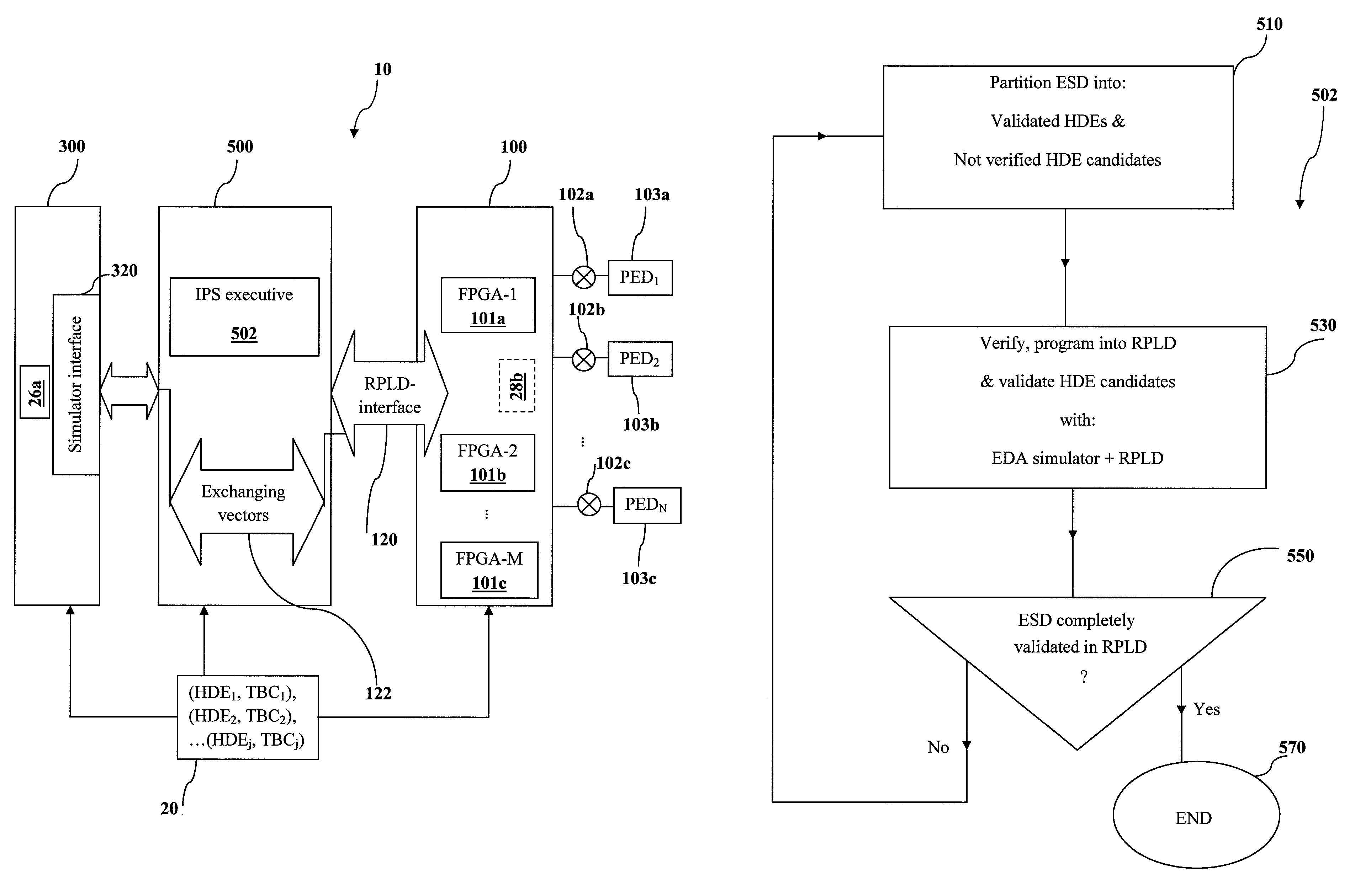
[0066]FIG. 1 illustrates an overall top level architecture of IPS 10, according to one embodiment of the present invention, for a user to verify and validate an electronic system design (ESD) 20 with its design data represented by hierarchical design elements (HDEs). Each HDE includes its own corresponding test bench (TBC). In FIG. 1, the HDEs and their respective associated TBCs are labeled (HDE1, TBC1), (HDE2, TBC2), . . . , (HDEj, TBCj). As part of the ESD 20, the HDEs further interact with one another ac...


PUM


Abstract

An integrated prototyping system (IPS) is proposed for verifying and validating an electronic system design (ESD) with hierarchical design elements (HDEs). The IPS has: a) A reprogrammable logic device (RPLD) having an emulation timing base and an RPLD-interface for programming and simulating HDEs under validation while transacting exchanging vectors. The RPLD is also switchably coupled to numerous external peripheral electronic devices (PED), b) An EDA simulator for simulating then verifying selected HDEs while transacting exchanging vectors. The EDA simulator also has a simulator interface; and c) An IPS controller bridging the RPLD and the EDA simulator. The IPS controller has an IPS executive for progressively verifying and validating the ESD. The IPS executive further includes a co-emulation software for jointly and simultaneously running the RPLD and the EDA simulator with an event-based synchronization scheme for interchanging exchanging vectors on demand between the RPLD and the EDA simulator.

Description

CROSS REFERENCE TO RELATED APPLICATIONS[0001]The present invention is a Continuation-In-Part (CIP) of copending U.S. patent application (“Copending Application”), entitled “Method of Progressively Prototyping and Validating a Customer's Electronic System Design,” by Thomas B. Huang and Chioumin M. Chang, filed on Dec. 10, 2007, Ser. No. 11 / 953,366, and assigned to “INPA Systems, Inc. The Copending Application is hereby incorporated herein by reference in its entirety for all purposes.FIELD OF INVENTION[0002]The present invention relates generally to design / validation apparatus and method for designing complex electronic circuits. In particular, the present invention is directed to a prototyping system for verifying and validating electronic circuit designs that are particularly applicable to an ultra large scale integrated circuit type electronic circuit.BACKGROUND OF THE INVENTION[0003]As their level of integration continues its advancement, many complex electronic logic systems ca...

Claims


Application Information

Patent Timeline
13 Mar 2012
Publication
US8136065B2
IPC
G06F17/50
CPC
G06F17/5027; G06F2217/86; G06F30/331; G06F2117/08
Inventors
HUANG, THOMAS B.; CHANG, CHIOUMIN M.