Manufacturing method of thin film transistor using oxide semiconductor

a manufacturing method and technology of oxide semiconductor, applied in the direction of logic circuits, solid-state devices, pulse techniques, etc., can solve the problems of oxide semiconductor layer damage, resistance reduction, transistor cannot be turned off, etc., and achieve excellent transistor characteristics

Inactive Publication Date: 2012-06-05
CANON KK
View PDF47 Cites 187 Cited by
  • Summary
  • Abstract
  • Description
  • Claims
  • Application Information

AI Technical Summary

Benefits of technology

[0013]By following the present invention, it is possible to provide a thin film transistor having excellent transistor characteristics in ohmic contact for connecting the source electrode and the drain electrode by reducing a contact region with the electrode of an oxide semiconductor layer in resistance.

Problems solved by technology

However, in the above descried conventional technology, as a configuration of the thin film transistor, the ohmic contact layer and the like are not provided, and depending on the selection of electrode materials, there is a problem that comes from non-ohmic contact nature with the oxide semiconductor and the source electrode as well as the drain electrode.
When the insulation film is formed on the oxide semiconductor layer in the atmosphere not including the oxidized gas, the oxide semiconductor layer receives damages and is reduced in resistance to such an extent that the thin film transistor is unable to be turned off.

Method used


Image

  • Manufacturing method of thin film transistor using oxide semiconductor
  • Manufacturing method of thin film transistor using oxide semiconductor
  • Manufacturing method of thin film transistor using oxide semiconductor

Examples


examples

[0104]Hereinafter, the examples of the present invention will be described by using the drawings. However, the present invention is not limited to the following examples.

first example

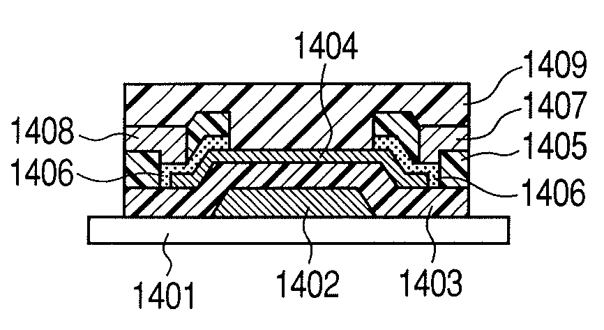
[0105]In the present example an inversely staggered (bottom gate) type MISFET element was fabricated. First, by using a photolithography method and a lift-off method, a gate terminal of Ti 5 nm / Au 40 nm / Ti 5 nm was formed on a glass substrate. Further, on that gate terminal, an insulation layer of a-SiOx was formed in thickness of 200 nm by the sputtering method. At that time, a SiO2 target was used for a sputtering target, and Ar gas was used for a sputtering gas. On the insulation layer, an amorphous oxide semiconductor film used as a semiconductor layer was formed in thickness of 20 nm at the room temperature by a sputtering method. The formation of the channel region employed the photolithography method and a wet etching by hydrochloric acid. After that, Ti 5 nm / Au 40 nm / Ti 5 nm was deposited by an electron beam vapor deposition method, and by the photolithography method and the lift-off method, source and drain terminals were formed. Further, as a second insulation film, a insu...

second example

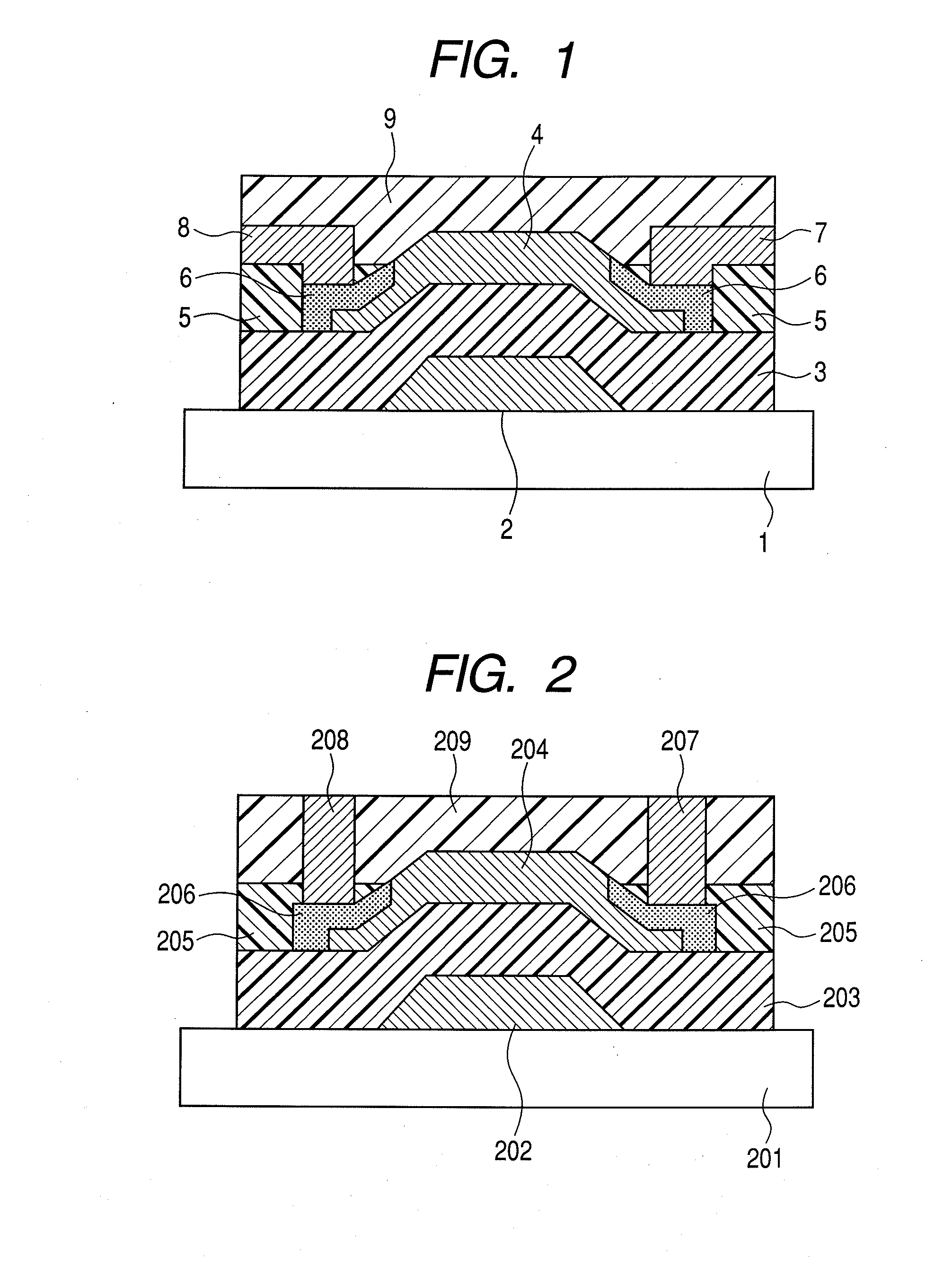
[0107]In the present example, an inversely staggered (bottom gate) type MISFET element was fabricated as similar to the first example except for the formation condition of a second insulation film.

[0108]As the second insulation film, an insulation layer by a-SiOx by a sputtering method was formed in the thickness of 100 nm. At that time, as a sputtering gas, an oxide atmosphere of an O2 / Ar mixed gas ratio 10% was used. In this manner, nine pieces of the inversely staggered (bottom gate) type MISFET elements shown in FIG. 12 were completed.

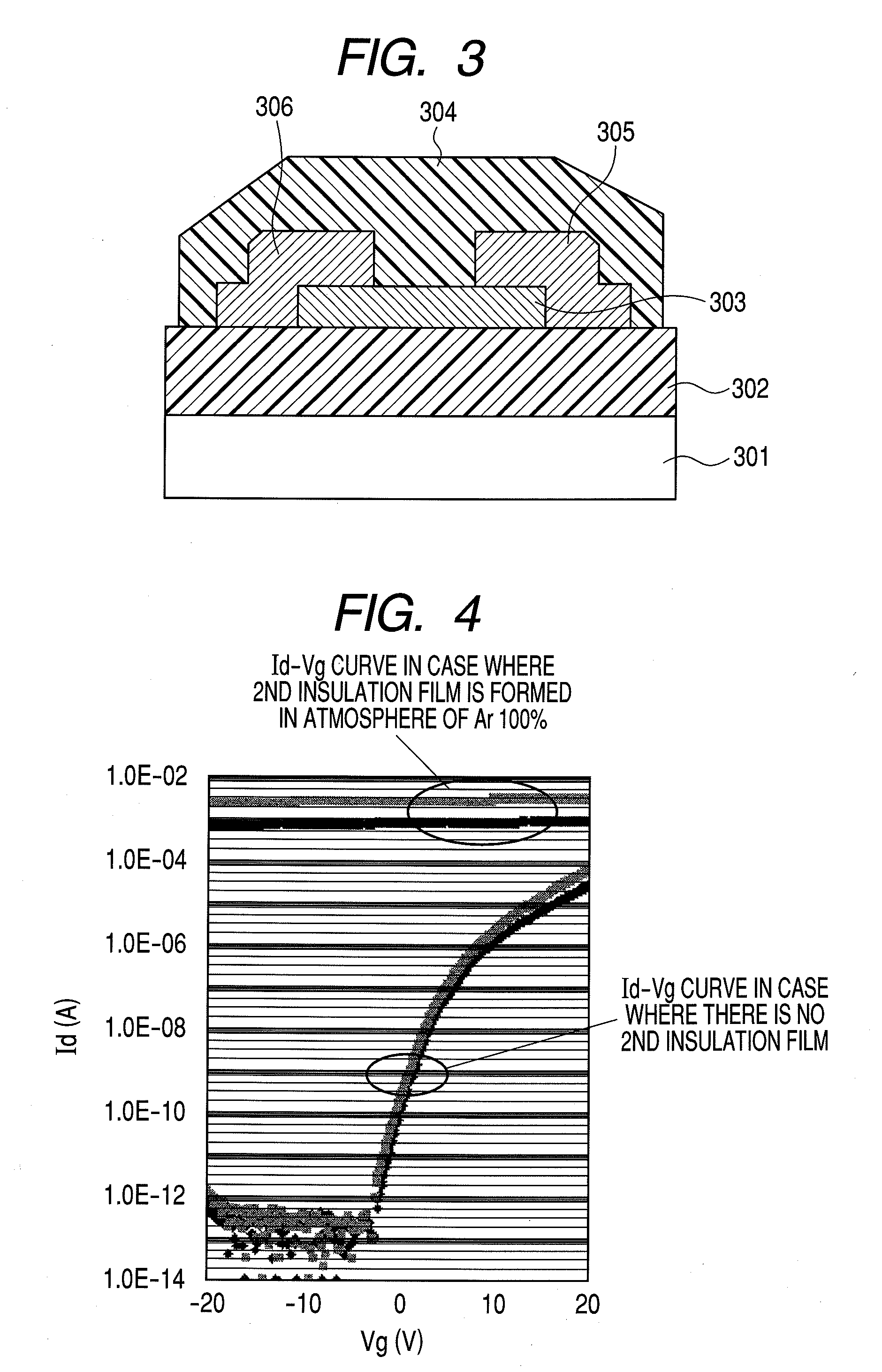
[0109]At the same time, under the same process condition, an oxide semiconductor conductivity measurement TEG element was fabricated, and the conductivity of the oxide semiconductor layer was measured. Von is a gate applied voltage at the rise time of a drain current (Id) in the transfer characteristic of a thin film transistor. A relation between the Von and the conductivity of the oxide semiconductor is shown in FIG. 10. Further, the second insul...


PUM


Abstract

A manufacturing method of a thin film transistor having at least a gate electrode, a gate insulation film, an oxide semiconductor layer, a first insulation film, a source electrode, a drain electrode, and a second insulation film on a substrate, including: forming the gate electrode on the substrate; forming the gate insulation film on the gate electrode; forming a semiconductor layer including amorphous oxide on the gate insulation film; patterning the gate insulation film; patterning the oxide semiconductor layer; reducing the oxide semiconductor layer in resistance by forming the first insulation film on the oxide semiconductor layer in the atmosphere not including an oxidized gas; patterning the first insulation film and forming a contact hole between the source electrode and the drain electrode and the oxide semiconductor layer; forming a source electrode layer and a drain electrode layer in the oxide semiconductor layer through the contact hole; forming the source electrode and the drain electrode through the contact hole and allowing the first insulation film to be exposed; patterning the exposed first insulation film and allowing a channel region of the oxide semiconductor layer to be exposed; and increasing the channel region in resistance by forming the second insulation film on the surface including the channel region of the oxide semiconductor layer in the atmosphere including an oxidized gas.

Description

TECHNICAL FIELD[0001]The present invention relates to a manufacturing method of a thin transistor film using an oxide semiconductor.BACKGROUND ART[0002]In recent years, in a thin film transistor used as a switching element of a display device such as an active matrix type liquid crystal display element or an organic electroluminescent element, the next generation thin film transistor has been actively developed. That is, the development of a thin film transistor using a transparent conductive oxide poly-crystal thin film mainly made of ZnO as a channel layer. This thin film is highly-mobile than amorphous silicon, and can be deposited at low temperature, and can form a flexible transparent thin film transistor on a substrate such as plastic plate and film. Further, since it is transparent for visible light, a shielding layer and the like are not required.[0003]An example of the manufacturing method of the thin film transistor mainly made of ZnO as described above will be described b...

Claims


Application Information

Patent Timeline
Patent Type & Authority Patents(United States)
IPC IPC(8): H03K19/094H03K19/0948
CPCH01L29/78618H01L29/7869H01L29/45
Inventor OMURA, HIDEYUKIHAYASHI, RYO
Owner CANON KK
Why Eureka
Try Eureka