Electronic-integration compatible photonic integrated circuit and method for fabricating electronic-integration compatible photonic integrated circuit

Active Publication Date: 2012-07-03
ELECTRONICS PHOTONIC IC INC EPIC INC
View PDF5 Cites 124 Cited by
  • Summary
  • Abstract
  • Description
  • Claims
  • Application Information

AI Technical Summary

Benefits of technology

[0034]Yet another object of the invention is to provide an EIC-PIC chip with the active photonic devices whose electrodes for n and/or p contact is made up of transparent conducting oxide (TCO) to enable effective electrical

Problems solved by technology

However, larger wafer size provides integration of many devices on the wafer, resulting in much lower cost of manufacturing per device.
A main challenge in photonic device integration is that photonic devices are typically large in size as compared to the electronic devices.
While ultra-large-scale integration of electronics has become a reality, the large-scale monolithic integration of high-performance photonic circuits on a chip is still largely unaccomplished.
Furthermore, current photonic int

Method used


Image

  • Electronic-integration compatible photonic integrated circuit and method for fabricating electronic-integration compatible photonic integrated circuit
  • Electronic-integration compatible photonic integrated circuit and method for fabricating electronic-integration compatible photonic integrated circuit
  • Electronic-integration compatible photonic integrated circuit and method for fabricating electronic-integration compatible photonic integrated circuit

Examples


Embodiment Construction

Overview of EIC-PIC:

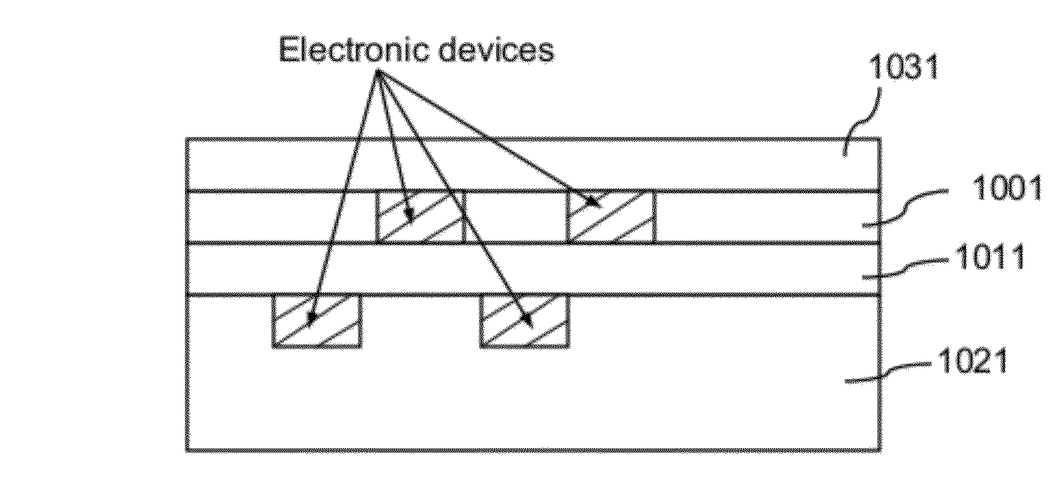
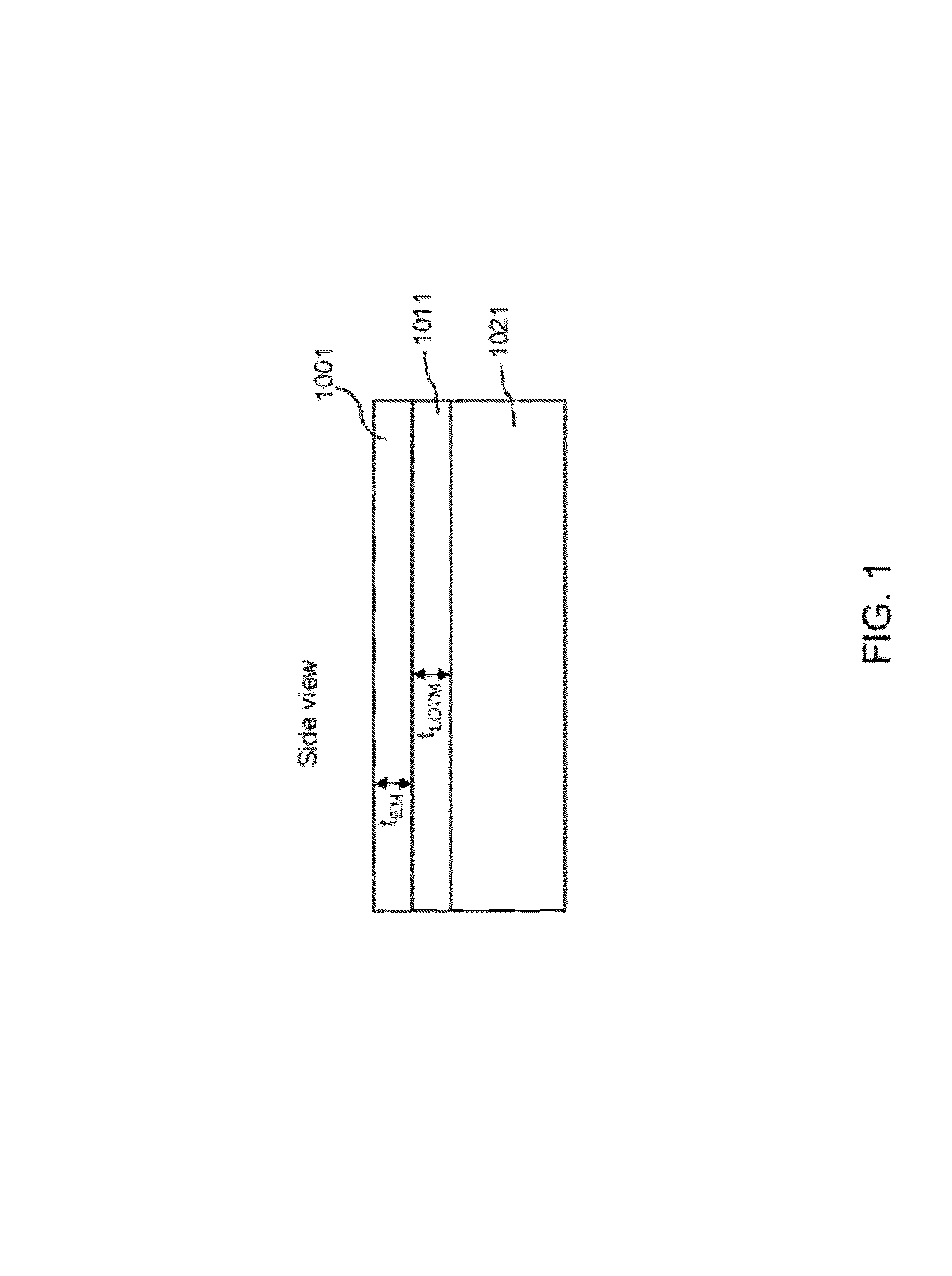
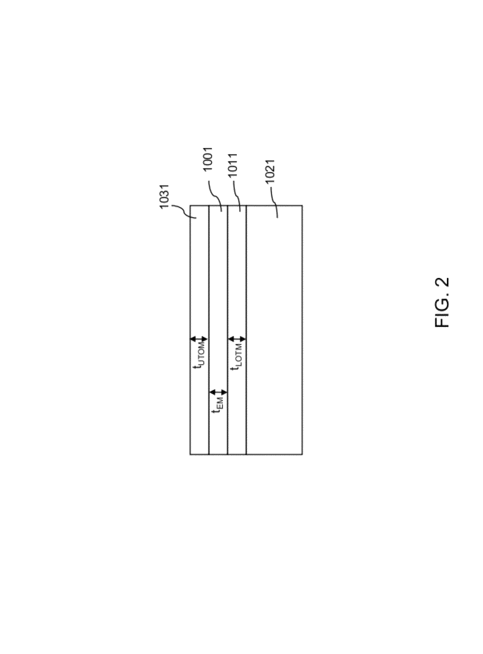
[0090]The present invention provides a method for the realization of Photonic / Nanophotonic Integrated Circuits that are compatible with electronic integration, referred to as electronic-integration compatible Photonic / Nanophotonic integrated circuit that will be referred to as EIC-PIC. An EIC-PIC shall have photonic devices integrated on a substrate using fabrication processes that are compatible with electronic integration processes.

[0091]Electronic Device Materials:

[0092]Electronic devices are typically fabricated on a layer of semiconductor material made up of silicon, GaAs, InP, or GaN substrate. The most commonly used material is Silicon. For illustration but not limitation, we will focus our discussion on the case of Silicon electronics integrated with photonic devices. Generalization to the utilization of other materials for electronics other than Silicon will be obvious to those skilled in the art.

[0093]Photonic Device Materials and Optical Wavelength:

[00...


PUM


Abstract

An electronic-integration compatible photonic integrated circuit (EIC-PIC) for achieving high-performance computing and signal processing is provided. The electronic-integration compatible photonic integrated circuit comprises a plurality of electronic circuit structures and a plurality of photonic circuit structures. The electronic and photonic circuit structures are integrated by a process referred to as monolithic integration. An electronic circuit structure includes one or more electronic devices and a photonic circuit structure includes one or more photonic devices. The integration steps of electronic and photonic devices are further inserted into standard CMOS process. The photonic circuit structures and the electronic circuit structures are integrated to form the electronic-integration compatible photonic integrated circuit device.

Description

REFERENCE TO RELATED APPLICATION[0001]This application claims the priority of U.S. provisional patent application, Ser. No. 61 / 200,315, filed Nov. 26, 2008, titled, ‘ELECTRONIC-INTEGRATION COMPATIBLE PHOTONIC INTEGRATED CIRCUIT AND METHOD FOR FABRICATING ELECTRONIC-INTEGRATION COMPATIBLE PHOTONIC INTEGRATED CIRCUIT’, the contents of which are herein incorporated by reference.FIELD OF THE INVENTION[0002]This invention relates generally to the field of Integrated Circuits and more specifically to Photonic Integrated Circuits that are compatible with Electronic Device Integration.BACKGROUND OF THE INVENTION[0003]An electronic Integrated Circuit (IC) is a device having integration of electronic circuits and components onto the surface of a substrate of a semiconductor material by processes of fabrication. The substrate materials include, but are not limited to, silicon (Si), Silicon on insulator (SOI), germanium (Ge), indium phosphide (InP), gallium arsenide (GaAs), gallium nitride (GaN...

Claims


Application Information

Patent Timeline
IPC IPC(8): G02B6/00H01L21/00
CPCG02B6/305G02B6/43G02F1/035G02F1/0311
Inventor HO, SENG-TIONGHUANG, YINGYAN
Owner ELECTRONICS PHOTONIC IC INC EPIC INC
Why Eureka
Try Eureka