Method for manufacturing a circuit board

a manufacturing method and circuit board technology, applied in the field of circuit boards, can solve the problems of difficult to form microfabricated wiring with a width of approximately 30 m or less, and achieve the effect of excellent reliability

Inactive Publication Date: 2012-09-11
TOYOTA JIDOSHA KK
View PDF22 Cites 6 Cited by
  • Summary
  • Abstract
  • Description
  • Claims
  • Application Information

AI Technical Summary

Benefits of technology

[0008]In the above manufacturing method, the protrusion pattern formed on the mold is directly transferred to the substrate side, and thus a recess with an arbitrary aspect ratio (i.e., the ratio of depth to width) can be formed on the substrate surface. As a result, a recess pattern that is microfabricated at a higher density can be formed on the substrate surface. In addition, pressure welding of the mold to the substrate surface results in simultaneous transfer of the protrusion pattern to the substrate surface and of a conductive material layer to the bottom face of each formed recess. Therefore, manufacturing processes can be simplified. Further, such pressure welding results in stable conditions of transferring of the conductive material layer to the substrate side.
[0009]A conductive material layer that is transferred to the bottom portion of each recess formed on a substrate is used as a base material to form a metal wiring in each recess. Thus, the circuit board of the present invention is obtained. As described above, the recess pattern formed on the substrate surface is microfabricated at a high density, and thus a circuit board with a high wiring density can be obtained. In the case of the circuit board of the present invention, the high-current flow through wiring portions can be resolved by determining a pattern comprising wirings with high aspect ratios. Thus, even when the circuit pattern is microfabricated (high-density formation), the circuit board of the present invention is not impaired in terms of insulating reliability when used as a mounting board.
[0019]The circuit board of the present invention is a high-density mounting board with excellent reliability, and thus it can be effectively used as an interposer, a rigid-flexible circuit board, and the like.
[0020]According to the present invention, it becomes possible to manufacture a circuit board having a further-microfabricated circuit pattern in further simplified steps.

Problems solved by technology

However, in the case of such subtractive method, it is difficult to form a microfabricated wiring with a width of approximately 30 μm or less.

Method used


Image

  • Method for manufacturing a circuit board
  • Method for manufacturing a circuit board
  • Method for manufacturing a circuit board

Examples


embodiment 1

(Embodiment 1)

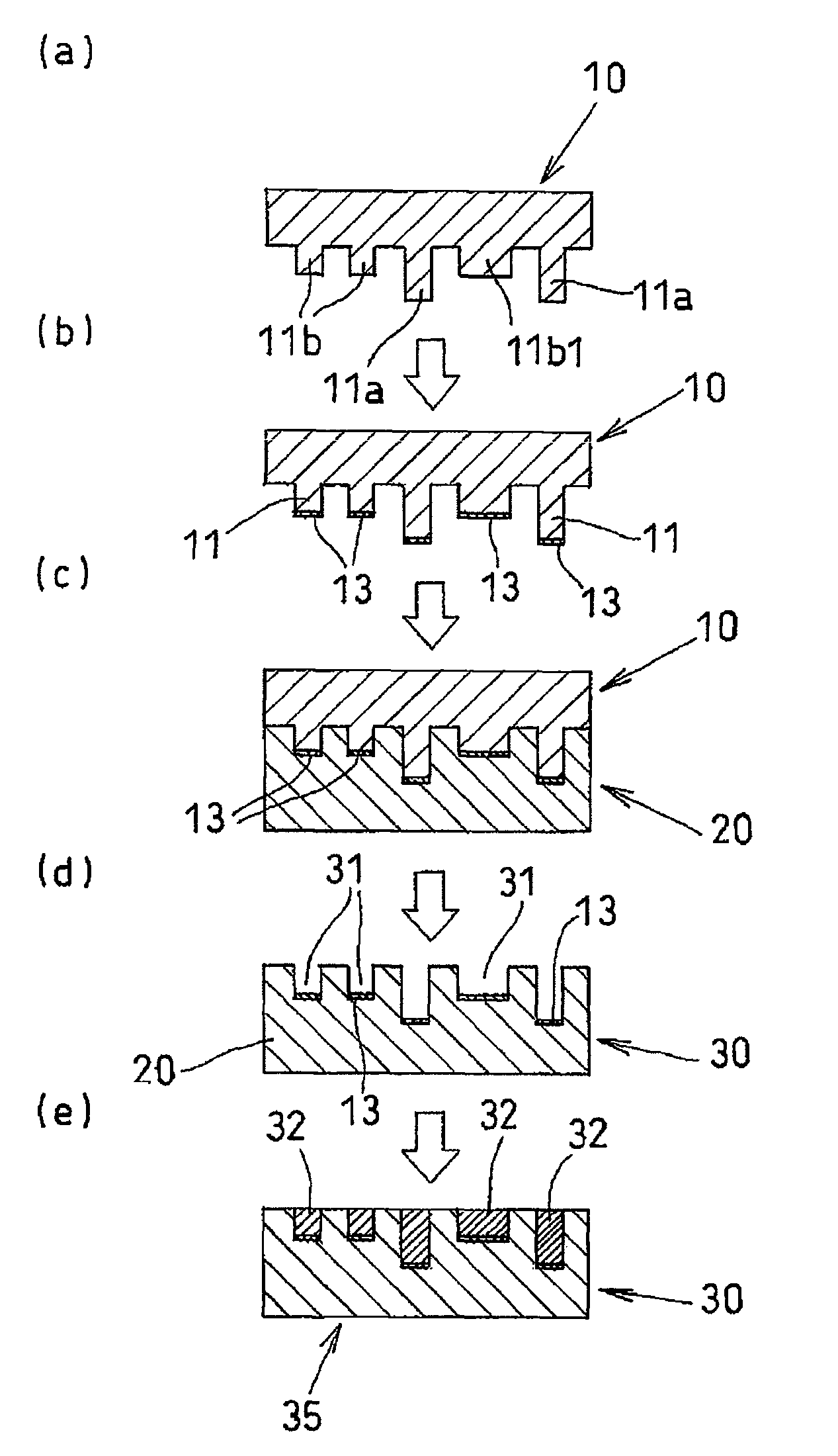
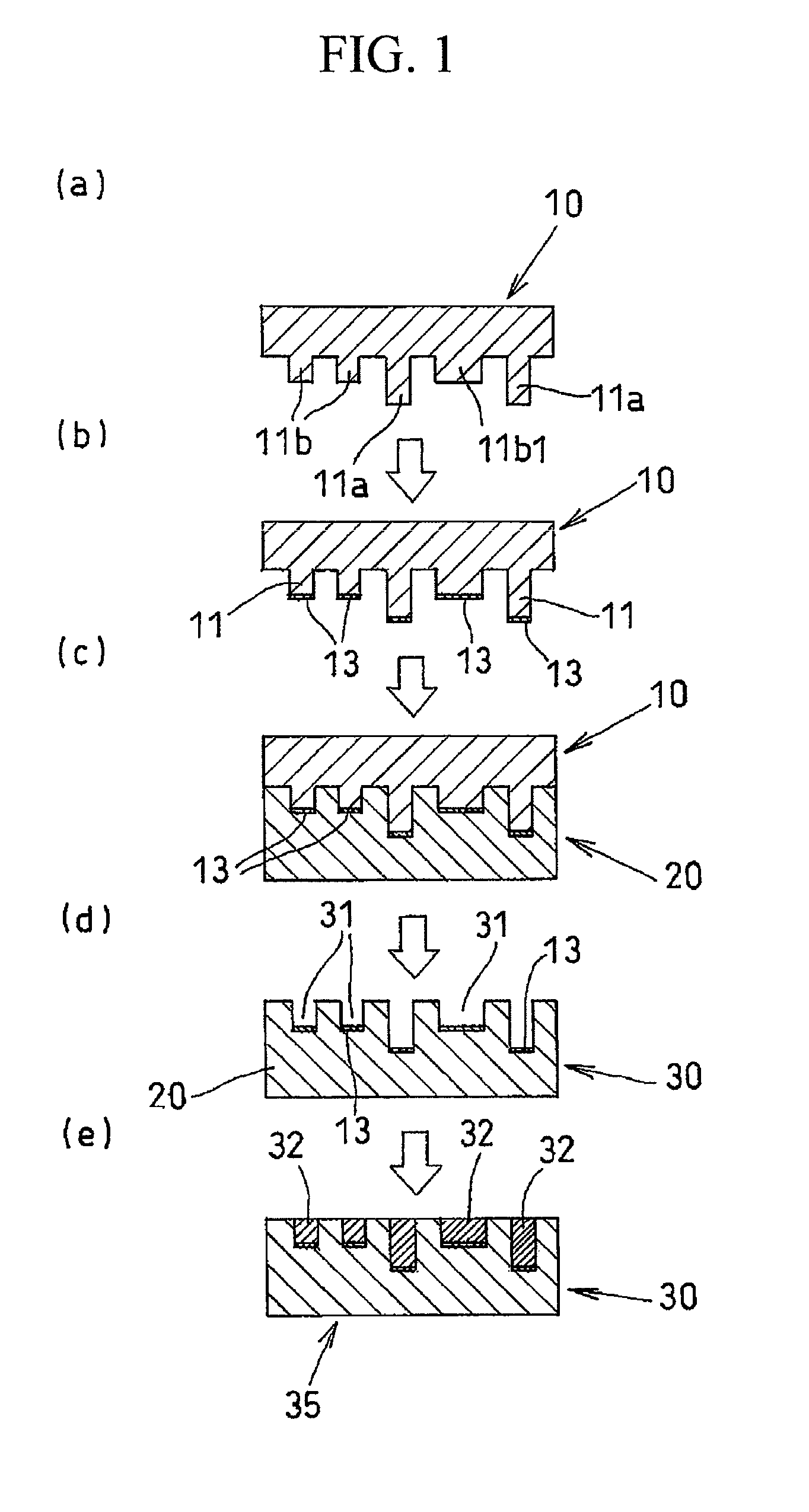
[0025]FIG. 1 shows a first embodiment of the method for manufacturing a circuit board of the present invention in the order of manufacturing steps. In FIG. 1, a numerical reference “10” denotes a mold. Protrusions 11 were formed on the flat face side of a nickel alloy plate having at least one flat face by a conventionally known electrocasting treatment such that they were formed in a pattern corresponding to a circuit pattern to be formed on the surface of a circuit board to be obtained. In the case of a mold 10 shown in FIG. 1a, protrusions 11a and 11b having different heights were formed in a manner such that a protrusion 11b1 has a greater width than the widths of the other protrusions 11b.

[0026]The widths of protrusions 11a and 11b were each determined to be 5 μm. The width of a protrusion 11b1 was determined to be 20 μm. The interval between each of the two protrusions was determined to be 5 μm. The heights of protrusions 11a and 11b were determined to be 15 μm ...

embodiment 2

(Embodiment 2)

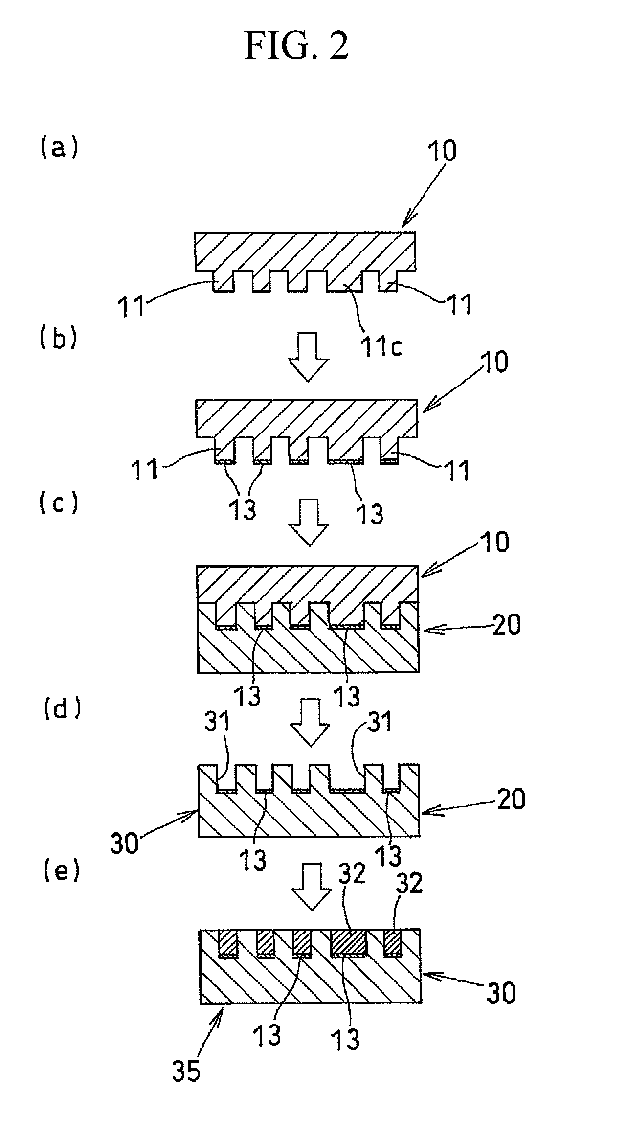
[0032]FIG. 2 shows a second embodiment of the method for manufacturing a circuit board of the present invention in the order of manufacturing steps. Herein, a glass plate having one flat face was used as a material for a mold 10 and a conventionally known sandblasting treatment was performed on the flat face side of the glass plate. Accordingly, protrusions 11 were formed as shown in FIG. 2a. The width and the height of each protrusion 11 were determined to be 5 μm and 10 μm, respectively, except that the width of a protrusion 11c was determined to be 10 μm. In addition, the interval between each of the two protrusions was determined to be 5 μm.

[0033]Next, a silver paste mainly consisting of silver nanoparticles with an average particle size of 20 nm was stretched and applied to a thickness of 2 μm to the surface of a PET plate with the use of a bar coater or the like. The protrusion-11 side of a mold 10 was pressed thereto. Accordingly, as shown in FIG. 2b, a mold 10 ...

embodiment 3

(Embodiment 3)

[0037]Protrusions each having a width of 50 μm and a height of 50 μm were formed with the use of a quartz plate having one flat face (not shown) as a material for a mold 10 in the same manner as in Embodiment 2. The interval between each of the two protrusions was determined to be 10 μm.

[0038]Next, a silver paste mainly consisting of silver nanoparticles with an average particle size of 5 nm was stretched and applied to a thickness of 5 μm to the surface of a PET plate with the use of a bar coater or the like. The protrusion-11 side of the mold 10 was pressed thereto. Accordingly, a mold 10 was obtained, such mold having the protrusions 11 with head portions to which the silver paste 13 had been applied.

[0039]A polycarbonate resin film with a thickness of 80 μm was placed on a glass plate. Then, the protrusion-11 side of the mold 10 was pressed thereto, followed by heat treatment in vacuo at 170° C. for 10 minutes.

[0040]The mold 10 was removed from the glass plate at o...


PUM

PropertyMeasurementUnit
widthaaaaaaaaaa
thicknessaaaaaaaaaa
aspect ratiosaaaaaaaaaa

Abstract

According to the present invention, a circuit board having a further-microfabricated circuit pattern that can be manufactured in further simplified steps is obtained. For such purpose, a mold 10, which has protrusions 11 formed in a pattern corresponding to a circuit pattern, is used to apply a conductive material layer (metal paste) 13 to head portions of the protrusions 11 of the mold 10. The mold is heat- and pressure-welded to the surface of a substrate 20 that is made of a resin film or the like. Accordingly, a pattern comprising the protrusions 11 and the conductive material layer (metal paste) 13 are transferred to the substrate 20. After transfer, the resin substrate (resin molding 30) is immersed in a copper sulfate plating bath for electrolytic plating treatment. Copper ions in the plating bath were deposited inside each recess 31 while the conductive material layer 13 is used as a base material for the formation of a metal wiring 32. A pattern of the recesses 31 transferred to the substrate-20 side is determined depending on a pattern comprising the protrusions 11 on the mold 10. Thus, a microfabricated high-density circuit pattern formed with metal wirings 32 having arbitrary aspect ratios can be obtained.

Description

TECHNICAL FIELD[0001]The present invention relates to a circuit board and a method for manufacturing the same. In particular, the present invention relates to a circuit board comprising a thin-film substrate that is formed with a resin material and the like and has the surface on which metal wirings are formed in a desired pattern, and it also relates to a method for manufacturing the same.BACKGROUND ART[0002]Dry processes involving vacuum evaporation, sputtering, and the like are known as methods for forming a microfabricated circuit pattern on the surface of a thin-film resin substrate. In addition, a subtractive method has been widely used, such method comprising: coating the entire surface of a substrate comprising, for example, a polyimide resin with a metal film comprising, for example, copper foil so as to produce a metal coating material; and removing unnecessary metal film portions by an etching treatment involving photolithography or the like. However, in the case of such ...

Claims


Application Information

Patent Timeline
Patent Type & Authority Patents(United States)
IPC IPC(8): H05K3/02
CPCH05K3/107H05K3/207H05K3/20H05K3/246H05K2201/0347Y10T29/49155H05K2203/0108Y10T29/49156Y10T29/49158Y10T29/49117H05K2201/09736B29C59/02
Inventor YANAGIMOTO, HIROSHIBESSHO, TAKESHINAWAFUNE, HIDEMIAKAMATSU, KENSUKE
Owner TOYOTA JIDOSHA KK
Why Eureka
Try Eureka