Production of VDMOS-transistors having optimized gate contact

a technology of gate contact and transistor, which is applied in the direction of transistors, electrical devices, solid-state devices, etc., can solve the problems of difficult use of only one mask layer for both contact hole types, and later consequences with respect to the reliability of transistors

Active Publication Date: 2012-09-18
X FAB SEMICON FOUNDRIES
View PDF6 Cites 1 Cited by
  • Summary
  • Abstract
  • Description
  • Claims
  • Application Information

AI Technical Summary

Benefits of technology

[0015]The claimed invention has the advantages that the additional first dielectric layer, which in some embodiments is provided as an oxide layer (silicon oxide substantially without other components, hereinafter this will be denoted as non-doped, for instance SiO2 formed from TEOS) that is formed on the non-patterned polysilicon that protects the source / polysilicon layer during the silicon etching of the source / body contact. The layer is then removed during the back etching of the intermediate isolating (dielectric) layer, after which an undisturbed homogeneous contact area of the polysilicon is provided within the gate contact holes.
[0016]A further advantage resides in the fact that the method for producing both contact systems may be performed by using a single mask (photo mask).

Problems solved by technology

In this case, the usage of only one mask layer for both contact hole types is difficult.
The problem resides in the fact that during the plasma etch process both contact hole types, i.e. the gate and the source / body contacts, are etched simultaneously.
The disadvantage of this technique resides in the fact that with the polysilicon being fully or partially removed in the gate contact hole the field oxide may be etched within the gate contact hole simultaneously.
In this manner, a deformed gate contact is formed, thereby possibly resulting in later consequences with respect to the reliability of the transistors.

Method used


Image

  • Production of VDMOS-transistors having optimized gate contact
  • Production of VDMOS-transistors having optimized gate contact
  • Production of VDMOS-transistors having optimized gate contact

Examples


Embodiment Construction

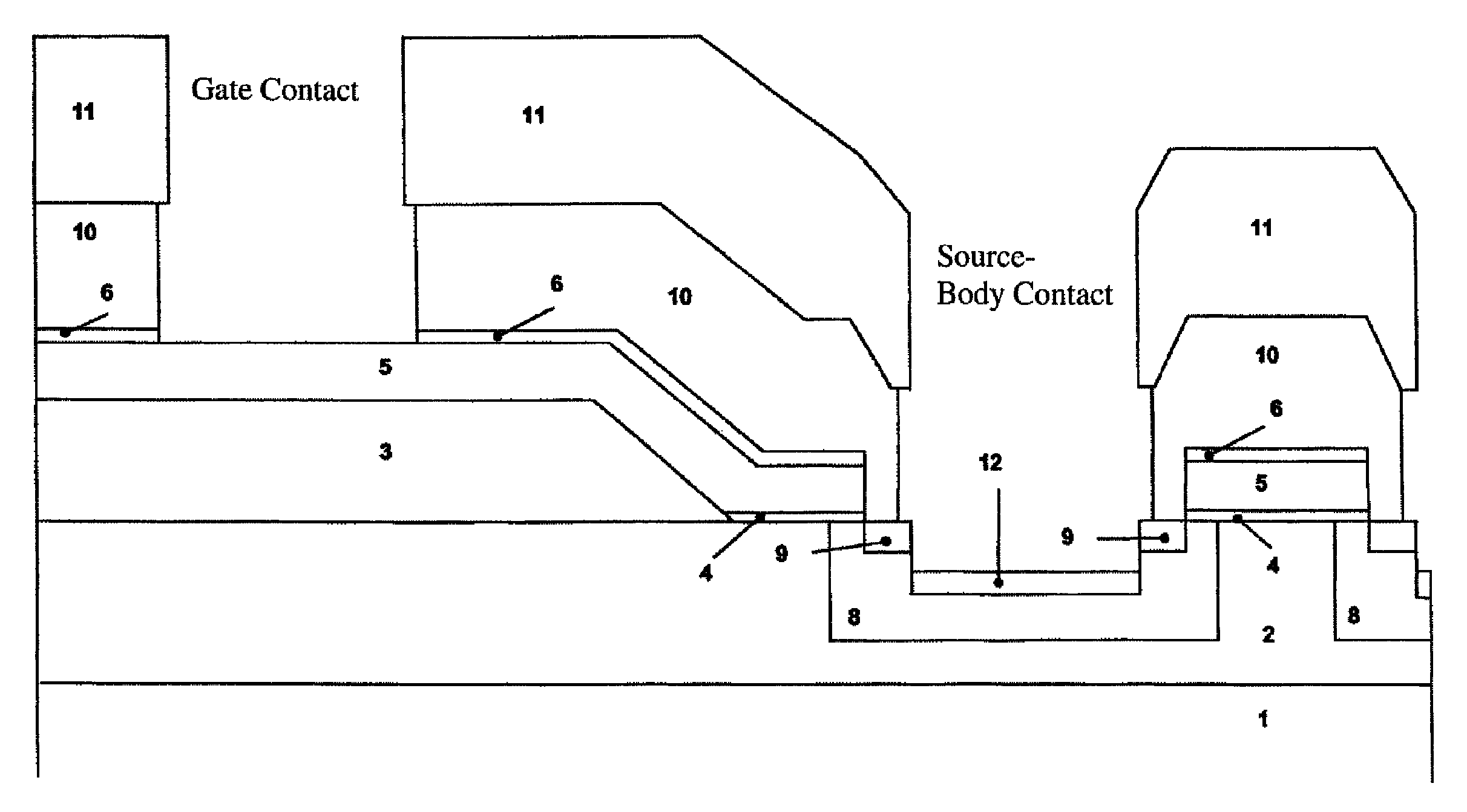
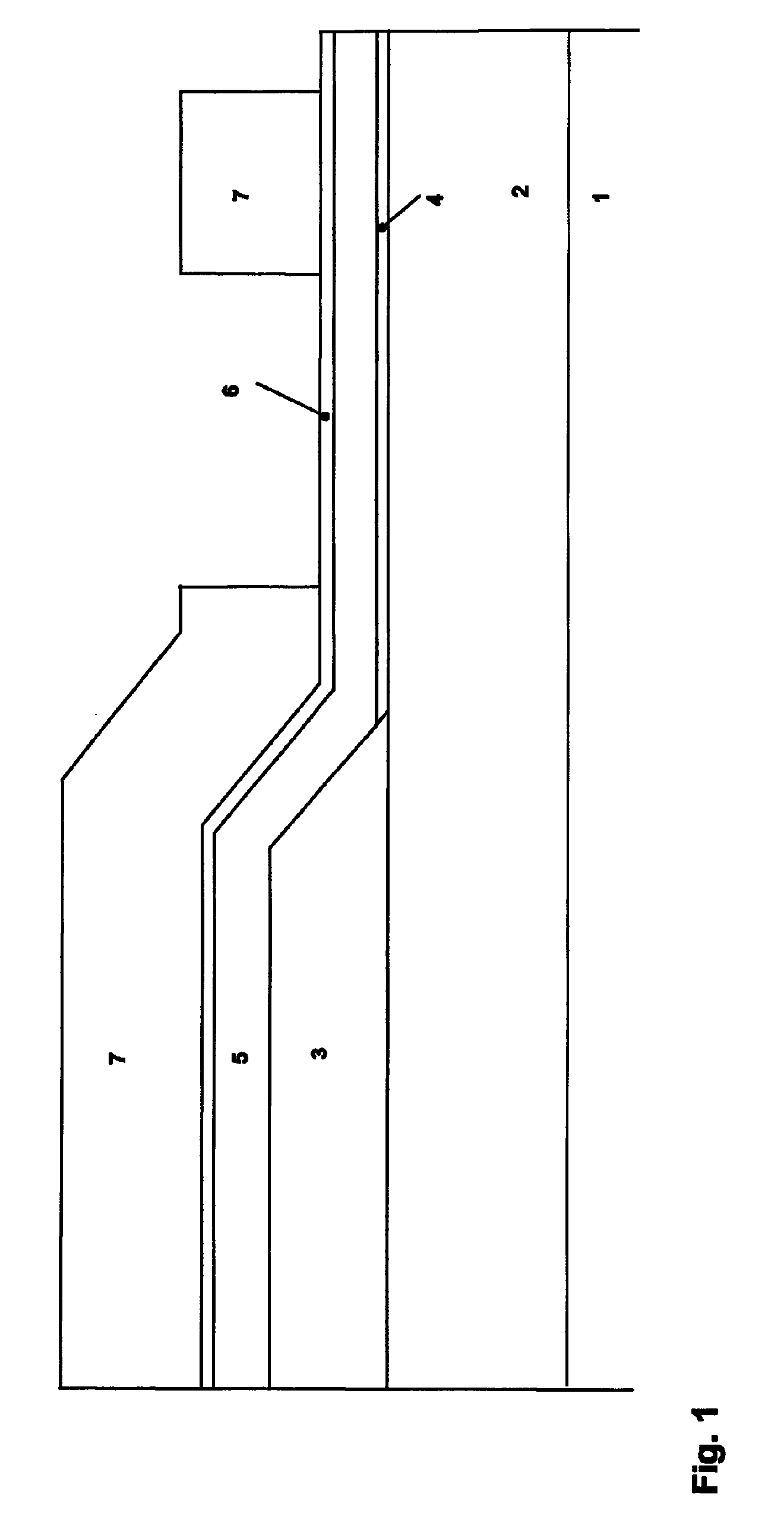
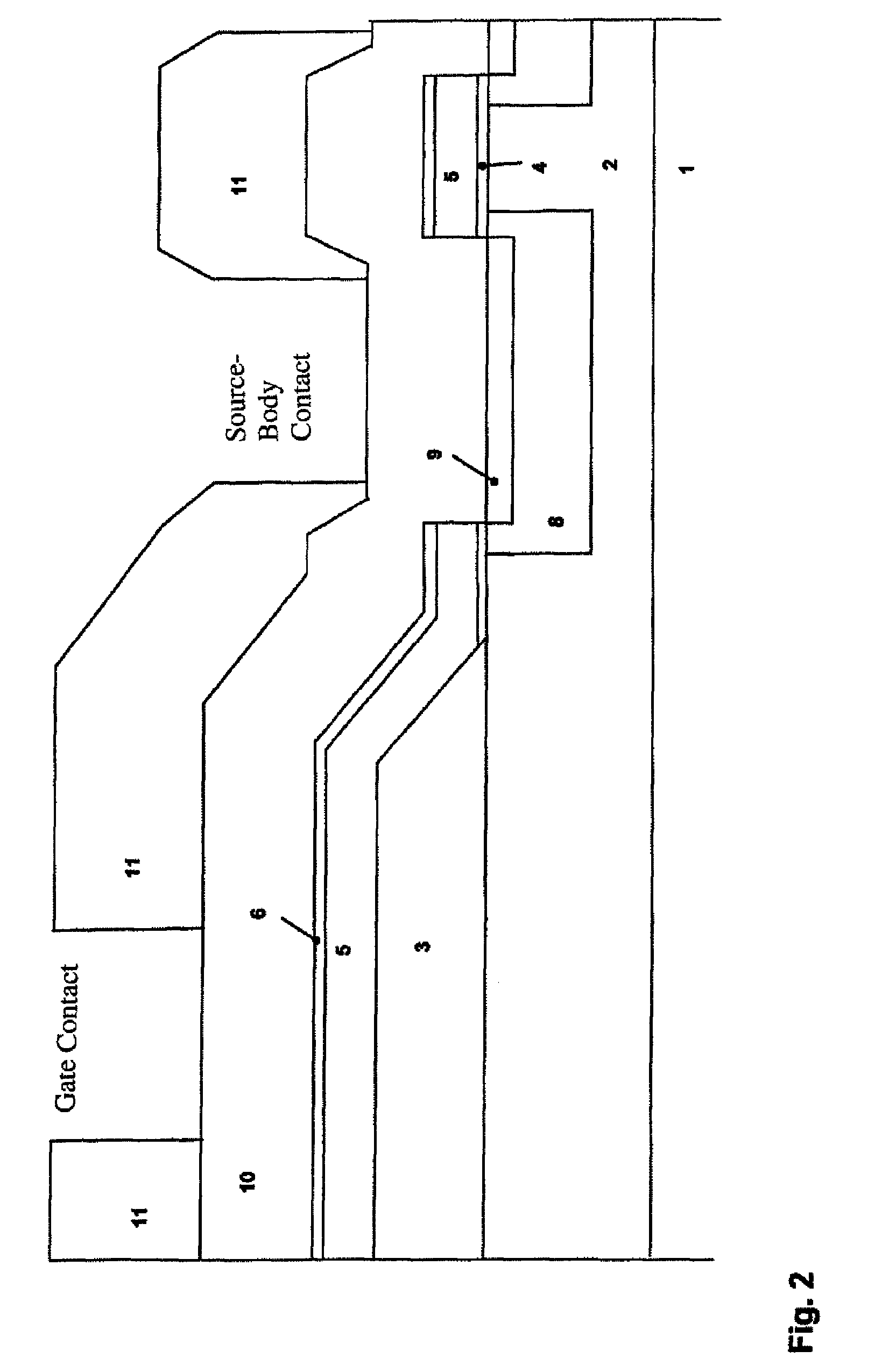
[0020]FIG. 1 illustrates the edge structure of VDMOS transistors and a VDMOS cell in an early stage of the technological process. In one embodiment the base material consists of a highly doped silicon wafer 1 including an epitaxy layer 2 of the same type of doping. A thick oxide layer 3, which is photolithographically patterned and etched, is grown on the epitaxy layer. The patterned oxide layer 3 has, in addition to the function of defining the surface area of the VDMOS cells, also the function to reduce the drain voltage with respect to the chip surface and to form a buffer layer between the epitaxy layer 2 and the gate contact layer. After forming the gate oxide 4 the deposition and doping the polysilicon layer 5 as a gate contact layer a first dielectric layer 6, for instance in the form of an “non-doped” oxide layer, for instance on the basis of TEOS, is deposited. It is formed with respect to layer thickness and etch rate such that it will completely be removed from the gate c...


PUM


Abstract

A method for producing VDMOS transistors in which a specific layer arrangement and a specific method sequence allow setting up an improved gate contact when simultaneously producing source and gate contacts using a single contact hole mask (photo mask).

Description

FIELD OF THE INVENTION[0001]The invention relates to a manufacturing method for VDMOS transistors (manufacturing) on a silicon substrate. The invention also relates to a thereby fabricated product in which the steps of the method are recognized.BACKGROUND OF THE INVENTION[0002]According to the prior art various technologies are used for the manufacturing of VDMOS transistors. A single VDMOS cell as a base element of the VDMOS transistors is sufficiently exhaustively described in the literature and is considered as well known. A substantial part of the manufacturing process is the contacting of a composite of VDMOS cells, in particular the manner of contacting the gate electrode.[0003]VDMOS cells are contacted at three locations. Firstly on the wafer back side or chip back side (across wide areas), respectively, and on the other hand at the wafer surface or chip surface at a restricted contact location. At the wafer surface or chip surface the gate and source / body contacts have to be...

Claims


Application Information

Patent Timeline
Patent Type & Authority Patents(United States)
IPC IPC(8): H01L21/66H01L21/336
CPCH01L29/66727H01L29/7811
Inventor DOEHNEL, JOCHENHERING, SIEGFRIED
Owner X FAB SEMICON FOUNDRIES
Why Eureka
Try Eureka