Semiconductor device and manufacturing method thereof

a semiconductor device and semiconductor technology, applied in the direction of semiconductor devices, basic electric elements, electrical appliances, etc., can solve the problem of limiting the use of transistors using oxide semiconductors as driver devices of semiconductor devices, and achieve excellent crystallinity, high field-effect mobility, and high performance.

Active Publication Date: 2012-10-23
SEMICON ENERGY LAB CO LTD
View PDF148 Cites 90 Cited by
  • Summary
  • Abstract
  • Description
  • Claims
  • Application Information

AI Technical Summary

Benefits of technology

[0010]An object of one embodiment of the present invention is to manufacture a transistor which can be formed over a larger substrate, includes an oxide semiconductor layer with excellent crystallinity to have a desirably high field-effect mobility, in order to realize commercialization of a large-sized display device, a semiconductor device with high performance, or the like.
[0012]As another method for increasing the field-effect mobility of a transistor, an oxide semiconductor layer is highly purified in the same step as or in a step different from a crystallization step. Specifically, the oxide semiconductor layer is highly purified by removing water or hydrogen which forms a donor level, reducing oxygen deficiency, and then sufficiently supplying oxygen that is a main component of the oxide semiconductor layer.
[0019]When the field-effect mobility of a transistor can be increased with any of the above manufacturing methods, for example, display characteristics can be improved by shortening switching time in a display device.

Problems solved by technology

However, there has been a limit to the use of a transistor using an oxide semiconductor as a driver device of a semiconductor device, for example, one switching element of a driver circuit of a large-sized display device or the like.

Method used


Image

  • Semiconductor device and manufacturing method thereof
  • Semiconductor device and manufacturing method thereof
  • Semiconductor device and manufacturing method thereof

Examples


embodiment 1

[0036]In Embodiment 1, a structure and a manufacturing method of a semiconductor device according to one embodiment of the disclosed invention will be described with reference to FIG. 1, FIGS. 2A to 2E, FIGS. 3A to 3D, and FIGS. 4A to 4E.

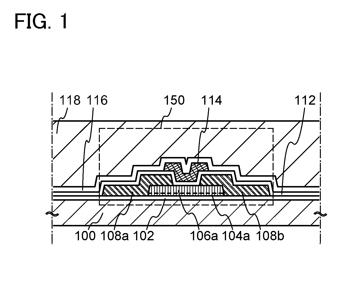
[0037]FIG. 1 is a cross-sectional view illustrating a transistor 150 which is an example of a structure of a semiconductor device. Note that the transistor 150 is an n-channel insulated gate field effect transistor (IGFET) whose carriers are electrons here; alternatively, a p-channel IGFET can be manufactured.

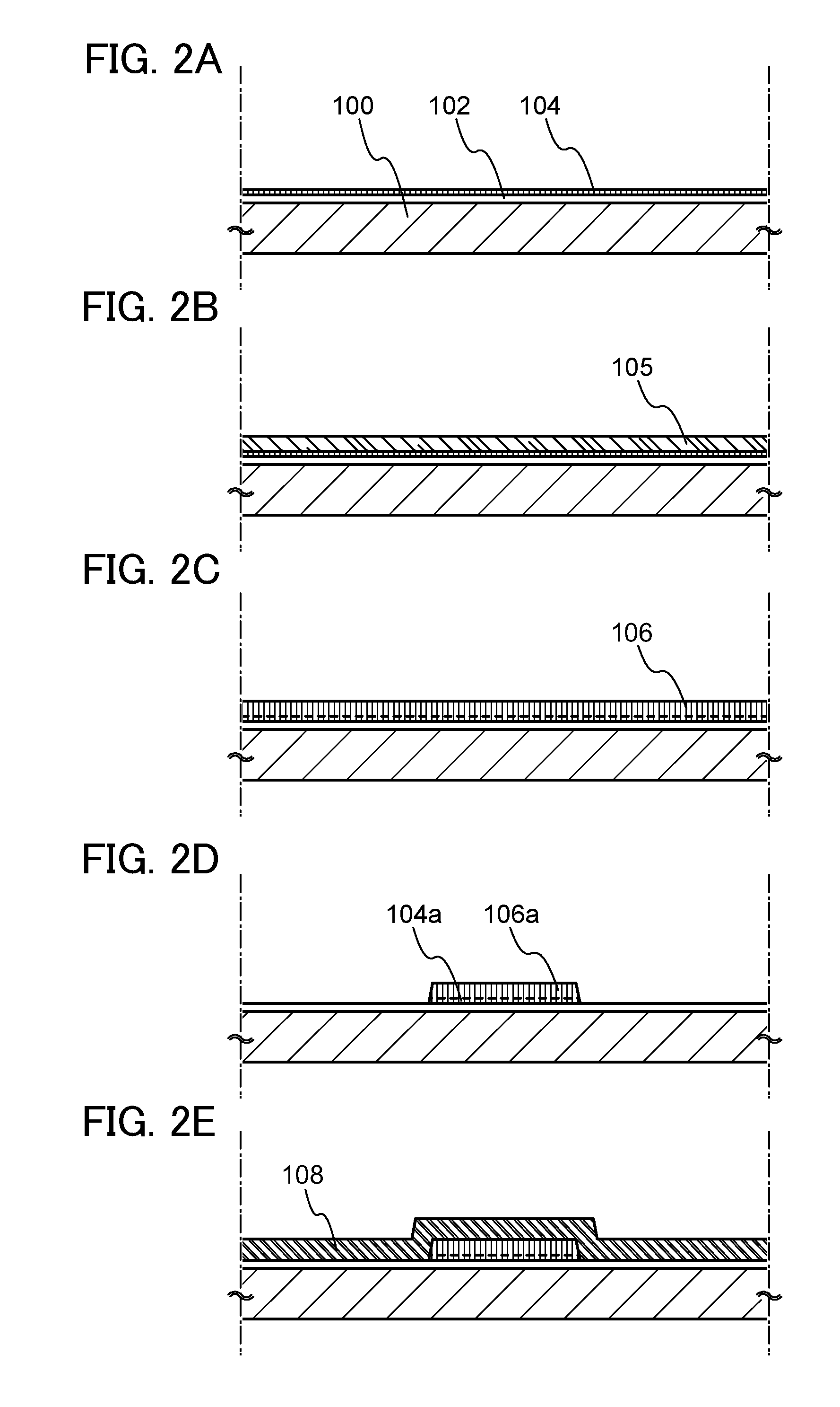
[0038]A manufacturing method of the transistor 150 will be described with reference to FIGS. 2A to 2E and FIGS. 3A to 3D.

[0039]First, an insulating layer 102 is formed over a substrate 100. Then, a first oxide semiconductor layer is formed over the insulating layer 102 and a region including at least a surface of the first oxide semiconductor layer is crystallized through first heat treatment, so that a first oxide semiconductor layer 104 is fo...

embodiment 2

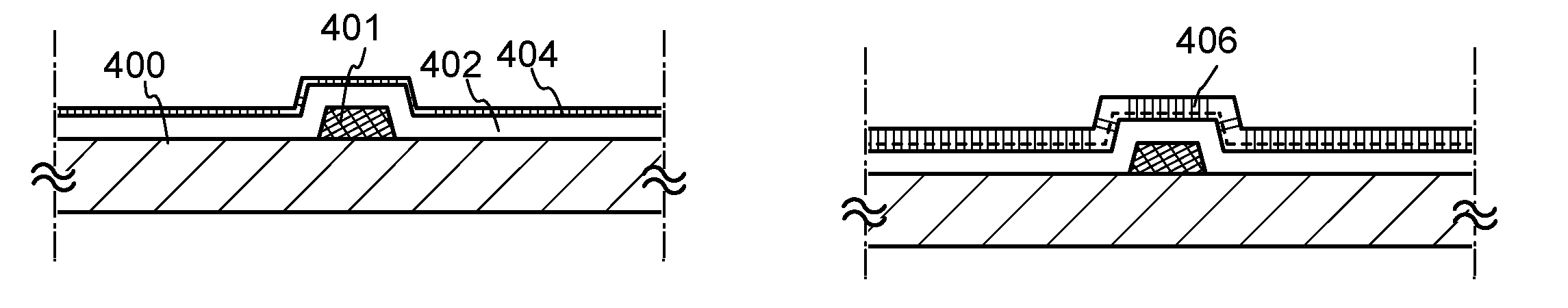
[0102]Although an example of manufacturing a top-gate transistor is described in Embodiment 1, an example of manufacturing a bottom-gate transistor is described in Embodiment 2.

[0103]First, a conductive film is formed over a substrate having an insulating surface, and then a gate electrode layer 401 is provided using a photolithography step with the use of a photomask.

[0104]As a substrate 400, a substrate of a glass material such as aluminosilicate glass, aluminoborosilicate glass, or barium borosilicate glass, a silicon substrate, a quartz substrate, or the like is used.

[0105]In Embodiment 2, a glass substrate is used as the substrate 400, and heat treatment at 650° C. for 6 minutes is performed twice on the substrate 400 because heat treatment is performed later for crystallization of an oxide semiconductor layer which is to be formed. By heating the substrate before the formation, film peeling or misalignment of a mask due to shrink of the substrate can be suppressed.

[0106]An ins...

embodiment 3

[0134]In Embodiment 3, an example of a channel stop transistor is shown with reference to FIG. 6.

[0135]Since Embodiment 3 is only partly different from Embodiment 2, detailed description is omitted here.

[0136]A procedure will be described below. Similarly to Embodiment 2, a gate electrode layer 501 and a gate insulating layer 502 are formed over a substrate 500; a first oxide semiconductor layer is formed, and first heat treatment is performed to crystallize the first oxide semiconductor layer; and a second oxide semiconductor layer is formed, and second heat treatment is performed to crystallize the second oxide semiconductor layer.

[0137]Next, an oxide insulating layer is formed and third heat treatment is performed. The oxide insulating layer is formed using the same material as that of the oxide insulating layer 412 described in Embodiment 2. In addition, the conditions of the third heat treatment are the same as those of the third heat treatment described in Embodiment 2, and ox...


PUM


Abstract

One embodiment of the present invention is to achieve high mobility in a device using an oxide semiconductor and provide a highly reliable display device. An oxide semiconductor layer including a crystal region in which c-axis is aligned in a direction substantially perpendicular to a surface is formed and an oxide insulating layer is formed over and in contact with the oxide semiconductor layer. Oxygen is supplied to the oxide semiconductor layer by third heat treatment. A nitride insulating layer containing hydrogen is formed over the oxide insulating layer and fourth heat treatment is performed, so that hydrogen is supplied at least to an interface between the oxide semiconductor layer and the oxide insulating layer.

Description

TECHNICAL FIELD[0001]The present invention relates to a semiconductor device having a circuit including at least a semiconductor element such as a transistor as one element, and a manufacturing method thereof. For example, the present invention relates to a power device which is mounted on a power supply circuit; a semiconductor integrated circuit including a memory, a thyristor, a converter, an image sensor, or the like; and an electronic appliance on which an electro-optical device typified by a liquid crystal display panel or a light-emitting display device including an organic light-emitting element is mounted as a component.[0002]Note that in this specification, semiconductor devices refer to all devices which can function by utilizing semiconductor characteristics, and electro-optical devices, semiconductor circuits, and electronic appliances are all included in the category of semiconductor devices.BACKGROUND ART[0003]Transistors formed over a glass substrate or the like have...

Claims


Application Information

Patent Timeline
Patent Type & Authority Patents(United States)
IPC IPC(8): H01L21/469H01L21/31H01L21/324H01L21/4763
CPCH01L21/3003H01L29/78693H01L29/7869H01L27/1225
Inventor YAMAZAKI, SHUNPEI
Owner SEMICON ENERGY LAB CO LTD
Why Eureka
Try Eureka