Integrated infrared sensors with optical elements, and methods

a technology of optical elements and infrared sensors, applied in the field of variable, can solve the problems of floating membrane support, thermocouple junctions over the cavity, and inability to accept a large number of device failures, and achieve the effect of small size and less cos

Active Publication Date: 2012-11-06
TEXAS INSTR INC
View PDF17 Cites 21 Cited by
  • Summary
  • Abstract
  • Description
  • Claims
  • Application Information

AI Technical Summary

Benefits of technology

[0033]It is an object of the invention to provide an IR radiation sensor which is substantially smaller and less expensive than the IR radiation sensors of the prior art.

Problems solved by technology

Such fragility ordinarily results in an unacceptably large number of device failures during subsequent wafer fabrication, subsequent packaging, and ultimate utilization of the IR sensor of FIGS. 1A and 1B.
Unfortunately, the floating membrane supporting one of the group of thermocouple junctions over the cavity as shown in FIG. 1 of Du and Lee (Prior Art FIG. 1A herein) is very fragile, because of the irregular sizes and spacings of the etchant openings and partly by the thinness of the dielectric layer 3.
The above described prior art IR sensors require large, expensive packages.
Furthermore, the “floating” portion of dielectric membrane 3 over cavity 4 in Prior Art FIG. 1A is quite fragile.
This creates a large opening span that is difficult to protect.
Alignment of a small thermopile sensor of the kind shown in the above mentioned Du and Lee article or included in the Melexis IR thermometer with a discrete collimating lens is difficult and expensive because of the relatively small size of the thermopile membrane.
The thermopile might have a dimension of only approximately 200 microns across, so misalignment of the discrete collimating lens by more than approximately 50 microns may result in substantial errors in focusing the incoming IR radiation onto the thermopile.
Furthermore, if the collimating lens is located a few centimeters from the thermopile, tilt of more than a few degrees of the plane of the collimating lens with respect to the plane of the thermopile will cause the focal point to be substantially misaligned with the thermopile.
The degree of precision alignment typically needed is achievable but quite costly using conventional alignment methods.

Method used


Image

  • Integrated infrared sensors with optical elements, and methods
  • Integrated infrared sensors with optical elements, and methods
  • Integrated infrared sensors with optical elements, and methods

Examples


Embodiment Construction

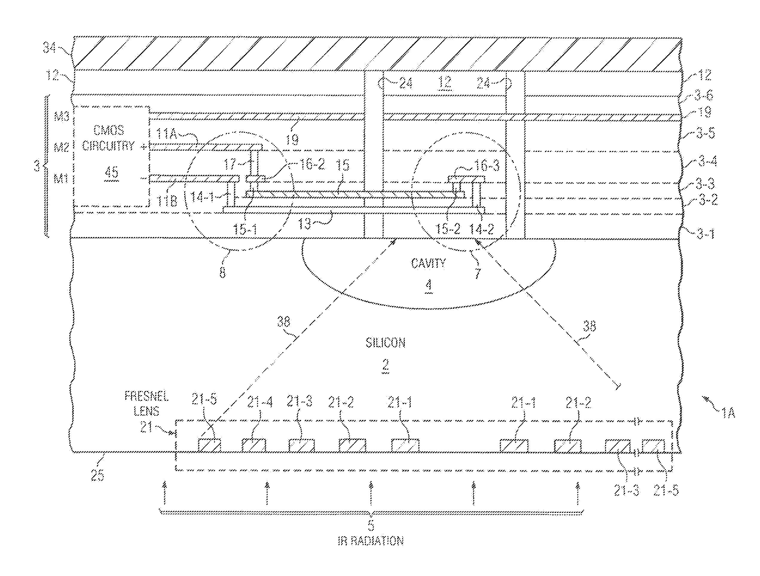
[0070]FIG. 3 shows a detailed cross-section of an integrated circuit IR sensor chip 1A which includes silicon substrate 2 and cavity 4 therein, generally as shown in FIG. 5 except that chip 1 as shown in FIG. 5 is inverted. Silicon substrate 2 includes a thin layer (not shown) of epitaxial silicon into which cavity 4 is etched, and also includes the silicon wafer substrate on which the original epitaxial silicon layer is grown. IR sensor chip 1 includes SiO2 stack 3 formed on the upper surface of silicon substrate 2. SiO2 stack 3 includes multiple oxide layers 3-1, 2 . . . 6 as required to facilitate fabrication within SiO2 stack 3 of N-doped polysilicon layer 13, titanium nitride layer 15, tungsten contact layers 14-1, 14-2, 15-1, 15-2, and 17, first aluminum metallization layer M1, second aluminum metallization layer M2, third aluminum metallization layer M3, and various elements of CMOS circuitry in block 45. (Note however, that in some cases it may be economic and / or practical t...


PUM


Abstract

An infrared (IR) radiation sensor device (27) includes an integrated circuit radiation sensor chip (1A) including first (7) and second (8) temperature-sensitive elements connected within a dielectric stack (3) of the chip, the first temperature-sensitive element (7) being more thermally insulated from a substrate (2) than the second temperature-sensitive element (8). Bonding pads (28A) on the chip (1) are coupled to the first and second temperature-sensitive elements. Bump conductors (28) are bonded to the bonding pads (28A), respectively, for physically and electrically connecting the radiation sensor chip (1) to corresponding mounting conductors (23A). A diffractive optical element (21,22,23,31,32 or 34) is integrated with a back surface (25) of the radiation sensor chip (1) to direct IR radiation toward the first temperature-sensitive element (7).

Description

[0001]This invention is related to the assignee's co-pending applications:[0002]Ser. No. 12 / 380,316, which is entitled “INFRARED SENSOR STRUCTURE AND METHOD, ” which was filed on Feb. 26, 2009, and which is incorporated herein by reference;[0003]Ser. No. 12 / 380,318, which is entitled “ON-CHIP CALIBRATION SYSTEM AND METHOD FOR INFRARED SENSOR” and filed on Feb. 26, 2009;[0004]Ser. No. 12 / 456,910, entitled “METHOD AND STRUCTURES FOR ETCHING CAVITY IN SILICON UNDER DIELECTRIC MEMBRANE” and filed on Jun. 24, 2009;[0005]Ser. No. 12 / 454,257 (now U.S. Pat. No. 8,026,177), which is entitled “SILICON DIOXIDE CANTILEVER SUPPORT AND METHOD FOR SILICON ETCHED STRUCTURES” and filed on May 14, 2009;[0006]Ser. No. 13 / 208,130, which is entitled “SILICON DIOXIDE CANTILEVER SUPPORT AND METHOD FOR SILICON ETCHED STRUCTURES” and filed on Aug. 11, 2011; and[0007]Ser. No. 13 / 208,098, which is entitled “SILICON DIOXIDE CANTILEVER SUPPORT AND METHOD FOR SILICON ETCHED STRUCTURES” and filed on Aug. 11, 2011...

Claims


Application Information

Patent Timeline
Patent Type & Authority Patents(United States)
IPC IPC(8): H01L31/058
CPCG01J5/02G01J5/024G01J5/04G01J5/046G01J5/08G01J5/0803G01J5/0806G01J5/12
Inventor LAZAROV, KALIN V.MEINEL, WALTER B.
Owner TEXAS INSTR INC
Why Eureka
Try Eureka