Optical modulation signal generating device and optical modulation signal generating method

a technology of optical modulation signal and generating device, which is applied in the direction of semiconductor amplifier structure, multiplex communication, semiconductor lasers, etc., can solve the problems of large capacity increase, laser frequency fluctuation, and high speed of optical fiber transmission

Active Publication Date: 2012-11-06
NIPPON TELEGRAPH & TELEPHONE CORP
View PDF16 Cites 4 Cited by
  • Summary
  • Abstract
  • Description
  • Claims
  • Application Information

AI Technical Summary

Benefits of technology

[0016]The optical modulation signal generating device restricts a fluctuation of a frequency modulation component converted by adjusting parameters of an amplitude component and a phase component in the frequency filter. An etalon filter may be used as the frequency filter.

Problems solved by technology

Caused by an explosive increase in transmission capacity due to recent prevalence of the Internet, a large capacity increase and high speeding in optical fiber transmission are demanding.
However, there exists a problem that at current modulating, a frequency fluctuation in lasing wavelength of a laser is generated in accordance with intensity of a modulation signal.
However, because of directly modulating the laser, there is a problem that an operation speed is limited by a relaxation oscillation frequency of the laser.
At present, in a commercialized laser the relaxation oscillation frequency is the order of 10 GHz and it is difficult to realize modulation speed higher than that.
Since this frequency fluctuation causes deterioration of the optical signal at an optical fiber propagation time of the optical signal, it is difficult to perform long-distance transmission with no relay.
In addition, there is a problem that the LN modulator is not suitable for integration with DFB-LD.

Method used


Image

  • Optical modulation signal generating device and optical modulation signal generating method
  • Optical modulation signal generating device and optical modulation signal generating method
  • Optical modulation signal generating device and optical modulation signal generating method

Examples


first embodiment

[0068]FIG. 4 shows the construction of an optical modulation signal transmitting system according to a first embodiment of the present invention. An optical modulation signal generating device 101 includes an optical source 102 for frequency-modulating an optical signal with an NRZ signal from a signal source and a frequency filter 103 connected to the output thereof and having a phase component. The optical signal outputted from the optical modulation signal generating device 101 propagates through an optical fiber 104 and thereafter, is received at a receiving device 105.

[0069]FIG. 5 shows intensity components of input and output optical signals of the frequency filter in the optical modulation signal generating device, and FIG. 6 shows frequency components. In FIGS. 5 and 6, symbol sequence of “1” and “0” from the signal source are shown together. In any of them, a broken line shows a waveform before transmission of the frequency filter 103 and a solid line shows a waveform after...

second embodiment

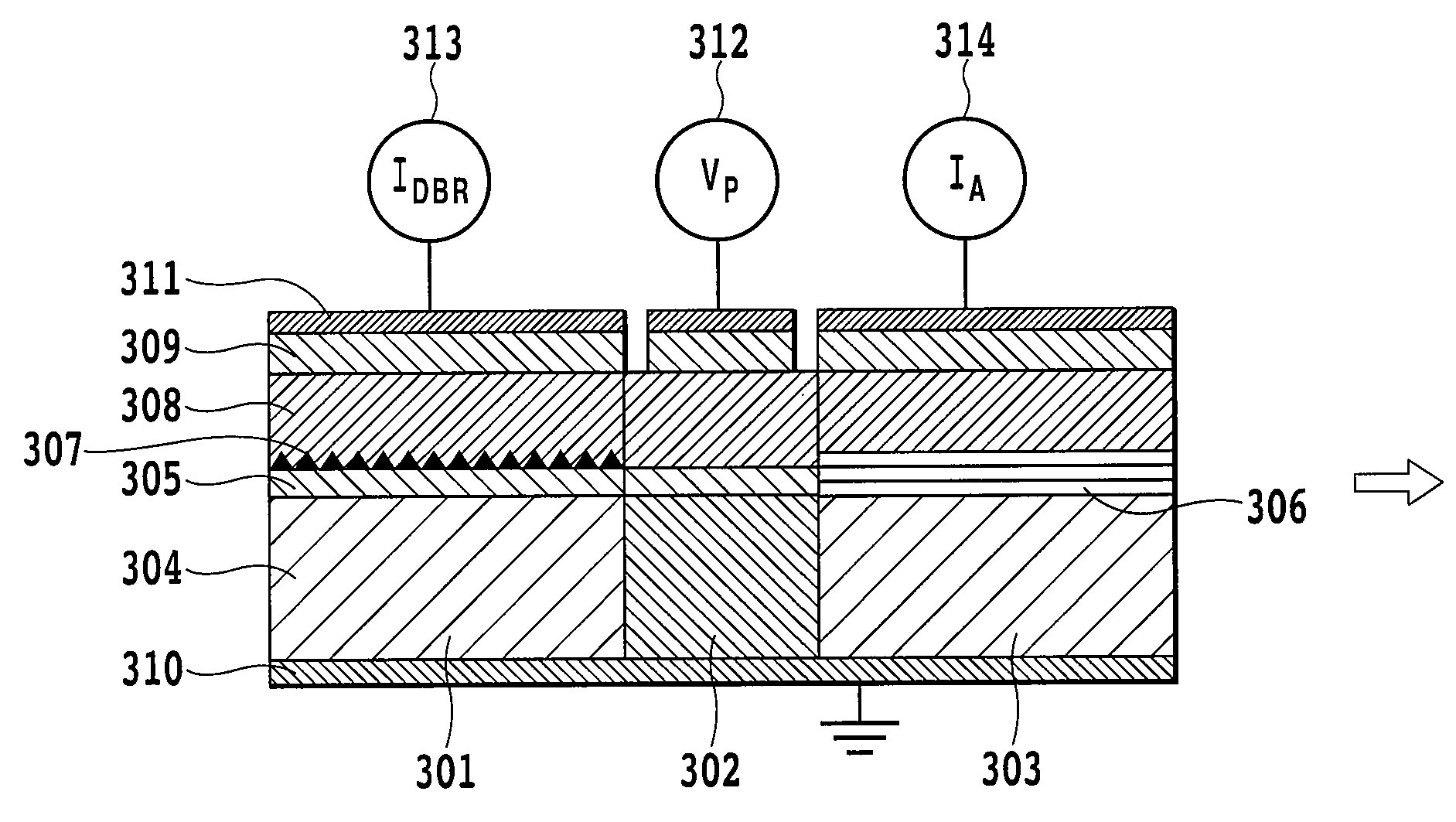
[0130]FIG. 23 shows the specific construction of an optical source according to a second embodiment. The optical source 102 is a distributed Bragg reflector laser including a DBR region 301a, the phase adjusting region 302, the active layer region 303, and a DBR region 301b toward an exit direction of light. The similar effect can be obtained even in the construction where the DBR region exists in both sides of the active layer and the phase adjusting region.

[0131]It should be noted that in the first and second embodiments, the adjustment of the lasing frequency can be realized even by a voltage drive in the DBR regions 301a and 301b. The similar effect can be obtained by voltage-driving the DBR regions 301a and 301b with lasing wavelength controlling voltage devices 313a and 313b.

third embodiment

[0132]FIG. 24 shows the specific construction of an optical source according to a third embodiment. The optical source 102 includes a coupled ring filter region 401, the phase adjusting region 302, and the active layer region 303 toward an exit direction of light. As similar to the first embodiment, the active region 303 is formed of a multiple quantum well layer and the phase adjusting region 302 is formed of a bulk or a quantum well waveguide layer.

[0133]The coupled ring filter region 401 includes a ring resonator 411a having a ring diameter of FSR 600 GHz and a ring resonator 411b having a ring diameter of FSR 700 GHz. The phase adjusting region 302 and the ring resonator 411a are coupled via a waveguide 412a by a 2×2 coupler 413a having a coupling constant of 0.5. The ring resonator 411a and the ring resonator 411b are coupled via a waveguide 412b by 2×2 couplers 413b and 413c each having a coupling constant of 0.5. Further, the ring resonator 411b is coupled to the waveguide 41...


PUM


Abstract

There is provided an optical modulation signal generating device in which an operation speed is not limited by a relaxation oscillation frequency of a laser, and high-speed modulation and long-distance transmission can be performed. The optical modulation signal generating device converts a signal from a signal source into an optical signal and outputs the optical signal to a transmission medium having frequency dispersion. The optical modulation signal generating device includes an optical source (102) for performing frequency modulation by the signal from the signal source to generate an optical signal having only a frequency modulation component, and a frequency filter (103) for converting the frequency modulation component of the optical signal into an intensity modulation component and a frequency modulation component.

Description

TECHNICAL FIELD[0001]The present invention relates to an optical modulation signal generating device and an optical modulation signal generating method, and in more detail to an optical modulation signal generating device and an optical modulation signal generating method for performing transmission at a high speed and in a long distance through an optical fiber.BACKGROUND ART[0002]Caused by an explosive increase in transmission capacity due to recent prevalence of the Internet, a large capacity increase and high speeding in optical fiber transmission are demanding. At present, an introduction of a system having a transmission speed of 10 Gbps is going forward in a backbone network, but for meeting a demand for further larger capacity, a transmitting system having a higher transmission speed is developing. For introducing a system having a transmission speed of more than 10 Gbps, it is important to further lower costs as compared to the system of 10 Gbps. Particularly in a signal so...

Claims


Application Information

Patent Timeline
Patent Type & Authority Patents(United States)
IPC IPC(8): H04B10/04H04B10/516H04B10/54H04B10/548
CPCH01S5/06256H04B10/516H04B10/541H04B10/548H01S5/005H01S5/0085H01S5/026H01S5/4087H01S5/50H04B2210/517
Inventor KAKITSUKA, TAKAAKIMATSUO, SHINJISEGAWA, TORUSUZUKI, HIROYUKI
Owner NIPPON TELEGRAPH & TELEPHONE CORP
Why Eureka
Try Eureka