Electrically isolated vertical light emitting diode structure

a vertical light and diode technology, applied in the field of vertical light emitting diodes and modules, can solve the problems of poor thermal performance of this kind of led grown on sapphire wafers, inability to drive this chip harder without significantly degrading lpw, and show a marked drop in efficiency, so as to improve thermal and/or electrical conductivity and low cost

Active Publication Date: 2012-11-13
LUMILEDS HLDG BV
View PDF5 Cites 11 Cited by
  • Summary
  • Abstract
  • Description
  • Claims
  • Application Information

AI Technical Summary

Benefits of technology

[0037]The present invention thus combines the electrical isolation advantage of lateral light emitting devices with the thermal and electrical current drive performance of the vertical type light emitting devices. The present invention electrically isolates a light emitting device with a vertical current path at the semiconductor wafer level processing step thus allowing for a simplification of the light emitting module packaging used for high brightness light emitting devices which also ultimately leads to reduced cost. This electrically isolated vertical LED (EIVL) approach has many other advantages as will be described.
[0070]In the light emitting modules of the present invention, the light emitting devices provide a greatly enhanced luminous efficiency and greater drive current capability through the use of the electrically isolated vertical structure with its superior thermal performance and greatly reduced packaging.
[0073]The die attach layer is important for providing the necessary physical attachment between the light emitting devices and the substrate. Any suitable material may be used. For example, the die attach layer may comprise a solder layer, which is formed using solder selected from a group which includes eutectic solder, solder alloy, solder pre-form and solder paste. Alternatively, the die attach layer may comprise a material selected from a group which includes epoxy adhesive, resin, thermoplastic, and silver glass. In addition, all materials may be in-filled to improve thermal and / or electrical conductivity.
[0074]In one embodiment the circuit layout board is a PCB, in which case the circuit layout board of the light emitting module may comprise a low cost standard PCB bonded to the metal substrate.
[0084]The encapsulation may comprise any suitable encapsulant, including resins, epoxies, PMMA, polymers, Silicones and inorganic materials. It is preferred that at least a part of the encapsulation comprises an embedded Phosphor. The Phosphor may comprise of single or multiple component materials. This increased refractive index of the encapsulant can be used for improved light extraction out of the light emitting device.
[0086]As will be appreciated by the skilled person, the present invention provides a means of allowing efficient continuous high power injection into a small format semiconductor light emitting device while ensuring that the semiconductor light emitting junction is maintained at a constant low temperature providing for maximum efficiency and the longest operating lifetimes. The light emitting module of the present invention allows the heat to be rapidly conducted away from the light emitting device through a high thermal conducting but electrically isolated substrate heat sink. As such, the invention allows the thermal resistance of the light emitting module to be reduced to below 0.5 K / W, when substrate materials such as, but not restricted to, metals, high performance ceramics or High Thermal Path (HTP) IMS-PCBs are used.

Problems solved by technology

The thermal resistance of Sapphire is high and, as a result, it is not possible to drive this chip harder without significantly degrading the LPW.
The thermal performance of this kind of LED grown on a sapphire wafer is poor as the thermal conductivity of sapphire is low at 40 W / (m·K) and the wafer is typically thick at 0.4 mm, thus creating a large thermal resistance path as high as 18 K / W.
Although the above steps help to improve thermal dissipation, when such LED devices are driven at more than 0.5 W electrical drive power, they show a marked drop in efficiency due to elevated p-n junction temperatures associated with heat build-up in the chip.
Another issue related to this kind of chip is the current crowding between and around the contacts 109 and 107 and their associated below optimum current injection into the complete light emitting area 104, all of which leads to further reduced efficiency.
All of these introduce additional parts, assembly complexity, cost and additional thermal interfaces.
However, if this type of IMS-PCB is used with the LED placed directly on the PCB, then high junction temperatures will occur, as the thermal load will not be able to spread adequately in the copper circuit layer.
Of course, all these layers of packaging create extra cost and extra interfaces that increase thermal resistance.
This is an important issue when typical metal, graphite or conductive plastic heat sinks are used to prevent the heat sink becoming electrically live.
This is an important issue if typical metal, graphite or conductive plastic heat sinks are used to prevent the heat sink becoming electrically live.
However, due to the high packing density of the LED cells the thermal dissipation adversely affects the efficient driving of such an AC LED device.

Method used


Image

  • Electrically isolated vertical light emitting diode structure
  • Electrically isolated vertical light emitting diode structure
  • Electrically isolated vertical light emitting diode structure

Examples


Embodiment Construction

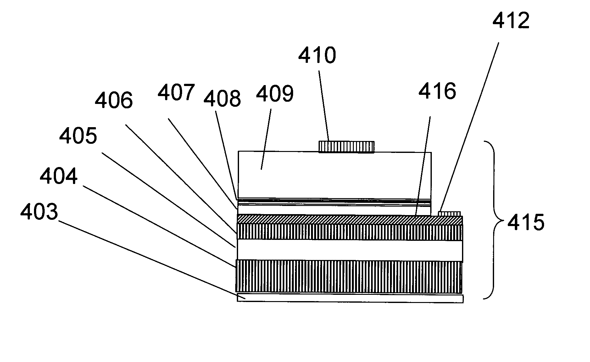
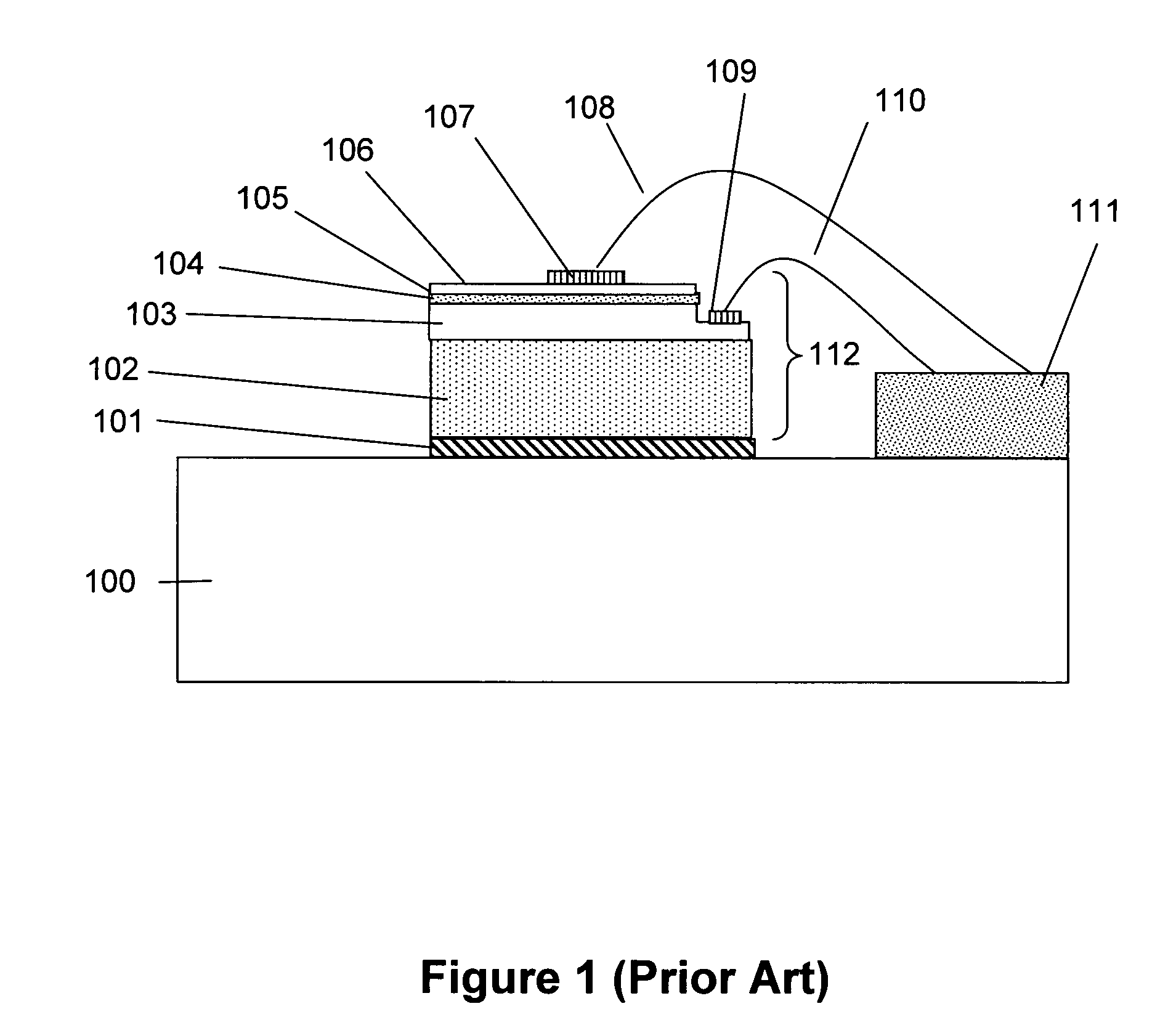
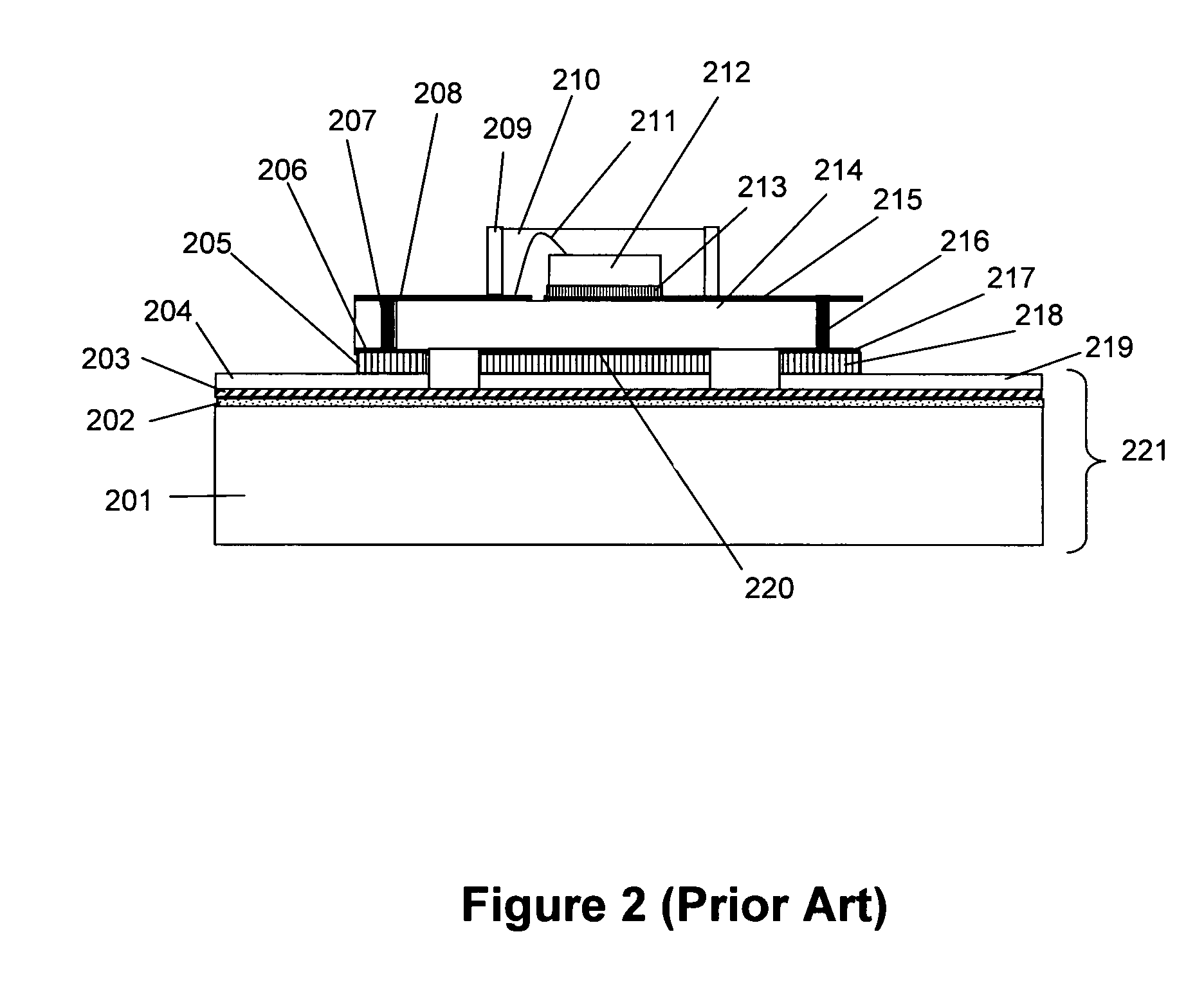
[0100]A key objective of the present invention is to provide a high luminous output semiconductor light emitting device while still maintaining high wall plug efficiency. The invention can be incorporated in a light emitting device based on any semiconductor material system. Examples of suitable semiconductor material systems include InGaN, InGaP, InGaAs, InP, or ZnO, but are not restricted to these. To illustrate the invention, a GaN based light emitting diode (LED) having an epitaxial layer formed on a sapphire substrate is used as an example. However, the application of the present invention is also not restricted to epitaxial layers grown on sapphire, and may include Si, SiC, Ge, native free-standing GaN, AlN, LiAlO or any other growth and substrate technology.

[0101]Another object of the invention is to make use of LEDs having a vertical current path, where the electrical current through the p- and n-doped materials is applied through substantially parallel contacts that allow t...


PUM


Abstract

A light emitting device is provided having high luminous output while maintaining high wall plug efficiency, wherein the high thermal and electrical conductivity paths of the device are separated during the semiconductor wafer and die level manufacturing step. The device includes an electrical conducting mirror layer, which reflects at least 60% of generated light incident on it, and an isolation layer having electrical insulating properties and thermal conducting properties. A first electrode, which is not in contact with the main semiconductor layers of the device, is located on the mirror layer. A light emitting module, system and projection system incorporating the light emitting device are also described, as is a method of manufacture of the device.

Description

[0001]This application is a national phase of International Application No. PCT / GB2008 / 003110 filed Sep. 12, 2008, and published in the English language as WO 2009 / 034349 on Mar. 19, 2009.FIELD OF THE INVENTION[0002]The present invention relates to a vertical light emitting diode and module with an improved thermal conductivity path and simplified packaging process.BACKGROUND TO THE INVENTION[0003]Light emitting diodes are based on a forward biased p-n junction. LEDs have recently reached high brightness levels that have allowed them to be used in new solid-state lighting applications, as well as replacements for high brightness light sources, such as light engines for projectors and automotive car headlights. These markets have also been enabled by the economical gains achieved through the high efficiencies of LEDs, as well as reliability, long lifetime and environmental benefits. These gains have been partly achieved by use of LEDs that are capable of being driven at high currents...

Claims


Application Information

Patent Timeline
Patent Type & Authority Patents(United States)
IPC IPC(8): H01L33/64H01L33/00H01L33/46H01L33/62
CPCH01L33/46H01L25/0753H01L33/0079H01L33/62H01L33/641H01L2224/45124H01L2224/85099H01L2224/48227H01L2224/49107H01L2224/73265H01L33/385H01L2924/01322H01L2224/45144H01L2924/01327H01L2224/48091H01L2924/00014H01L2924/00H01L2224/05599H01L2224/85399H01L2924/181H01L33/0093H01L2924/00012H01L33/64
Inventor MCKENZIE, JAMES STUARTZOOROB, MAJD
Owner LUMILEDS HLDG BV
Why Eureka
Try Eureka