Thermally enhanced electronic package utilizing carbon nanocapsules and method of manufacturing the same

a technology of carbon nanocapsules and electronic packages, applied in nanoinformatics, electrical apparatus construction details, casings/cabinets/drawers, etc., can solve the problems of increased power consumption, difficult dissipation of accumulated heat, and increased operating frequency, so as to reduce the operating temperature of electronic packages and improve thermal dissipation

Active Publication Date: 2012-12-25
CHIPMOS TECH INC
View PDF17 Cites 0 Cited by
  • Summary
  • Abstract
  • Description
  • Claims
  • Application Information

AI Technical Summary

Benefits of technology

[0010]One aspect of the present invention provides a thermally enhanced electronic package. A dielectric resin material mixed with carbon nanocapsules (CNC) is used in the electronic packaging to improve thermal dissipation. As the CNC transfers and dissipates heat into infrared energy through absorption and radiation, the CNC mixed material is effective for thermal dissipation and is thus capable of reducing the operating temperature of the electronic package.

Problems solved by technology

Continuous demand for improved performance of semiconductor products results in higher operating frequencies and greater power consumption.
In general, the insulating layers of the substrate 14 are polymers which also have poor thermal conductivity, so the accumulated heat is not easily dissipated from the insulating layers to the outside of the FBGA package 10.

Method used


Image

  • Thermally enhanced electronic package utilizing carbon nanocapsules and method of manufacturing the same
  • Thermally enhanced electronic package utilizing carbon nanocapsules and method of manufacturing the same
  • Thermally enhanced electronic package utilizing carbon nanocapsules and method of manufacturing the same

Examples


Embodiment Construction

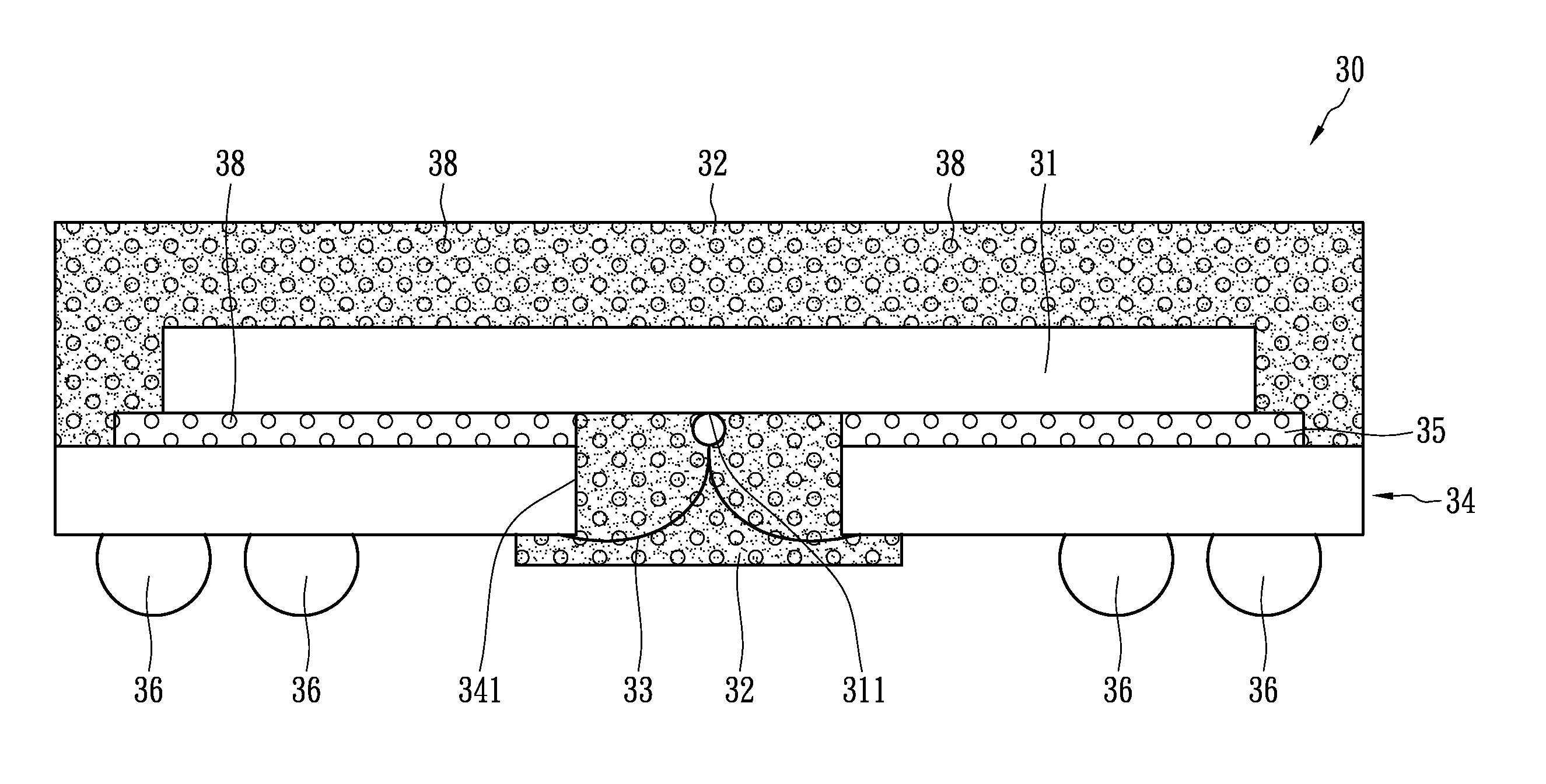
[0025]The invention relates to the application of carbon nanocapsules to semiconductor packages so that the semiconductor packages can have enhanced thermal dissipation characteristics. In particular, a dielectric material or resin is blended with a plurality of carbon nanocapsules for use in electronic packaging applications with the purpose of improving heat dissipation of semiconductor chips. Such a mixed material or resin is directly or indirectly in contact with semiconductor chips to improve heat transfer and dissipation. The mixed material can be applied in the portion of a semiconductor package such as flip chip underfill, non-flow underfill, chip encapsulant, chip coating, die-attach adhesives, non-conductive paste / film, conductive paste / film, film-on-wire, etc.

[0026]Carbon nanocapsules in the mixed material have the characteristic of effectively transforming heat into infrared radiation through absorption and radiation, which is the optimum method of heat removal from elec...


PUM


Abstract

A thermally enhanced electronic package comprises a chip, a substrate, an adhesive, and an encapsulation. The adhesive or the encapsulation is mixed with carbon nanocapsules. The substrate includes an insulation layer and a wiring layer formed on the substrate. The adhesive covers the chip and the substrate. The chip is electrically connected to the wiring layer. The encapsulation covers the chip and the substrate.

Description

CROSS REFERENCE TO RELATED APPLICATIONS[0001]This non-provisional application claims priority under 35 U.S.C. §119(e) of U.S. Provisional Application No. 61 / 354,927, filed Jun. 15, 2010, the entire contents of which are hereby incorporated by reference.BACKGROUND OF THE INVENTION[0002]1. Field of the Invention[0003]The present invention relates to a thermally enhanced electronic package, and more particularly, to an electronic package with high thermal dissipation capability.[0004]2. Description of the Related Art[0005]Continuous demand for improved performance of semiconductor products results in higher operating frequencies and greater power consumption. Therefore, electrical packages having high thermal conductivity capable of effective heat dissipation to reduce interconnect junction temperatures are needed for semiconductor products. One such electrical package is a type of semiconductor device called a liquid crystal display (LCD) driver. In addition, heat management solutions...

Claims


Application Information

Patent Timeline
Patent Type & Authority Patents(United States)
IPC IPC(8): H01L23/22H01L21/00H05K7/00
CPCB82Y10/00B82Y30/00H01L23/13H01L23/3128H01L24/29H01L25/0657H05K5/0213H05K7/205H01L23/49816H01L23/525H01L24/16H01L24/32H01L24/45H01L24/48H01L2224/16145H01L2224/16227H01L2224/29393H01L2224/32145H01L2224/32225H01L2224/456H01L2224/48091H01L2224/48227H01L2224/4824H01L2224/48465H01L2224/48471H01L2224/73204H01L2224/73215H01L2224/73265H01L2224/92147H01L2224/92247H01L2225/0651H01L2225/06541H01L2225/06565H01L2924/01013H01L2924/01014H01L2924/01029H01L2924/01033H01L2924/01077H01L2924/01082H01L2224/2919H01L2924/01005H01L2924/01006H01L2924/01074H01L2924/014H01L2924/0665H01L2224/29101H01L2224/16225B82B1/005Y10S977/932H01L2924/15311H01L2924/10253H01L2924/07802H01L2924/00014H01L2924/00H01L2924/00012H01L24/73H01L2924/14H01L2224/05008H01L2224/05022H01L2224/05001H01L2224/05569H01L2224/05572H01L2924/181H01L2224/8592H01L24/05H01L2224/05647H01L2224/05124H01L2224/05147
Inventor LIU, AN HONGWANG, DAVID WEI
Owner CHIPMOS TECH INC
Why Eureka
Try Eureka