Semiconductor device and peeling off method and method of manufacturing semiconductor device

a technology of semiconductor devices and semiconductors, applied in the field of peeling off a peeled off layer, can solve the problems of easy cracking and heavy, glass substrates and quartz substrates are difficult to be made larger, and cannot help lowering the highest temperature of the process

Inactive Publication Date: 2013-02-05
SEMICON ENERGY LAB CO LTD
View PDF175 Cites 227 Cited by
  • Summary
  • Abstract
  • Description
  • Claims
  • Application Information

AI Technical Summary

Benefits of technology

[0011]Moreover, the present invention aims at providing a peeling off method of peeling off without receiving the limitations such as the heating processing temperature, the kind of substrate or the like in the formation of the peeled off layer.
[0012]Moreover, the present invention aims at providing a semiconductor device weight-saved by pasting a peeled off layer on a variety of base members and its method of preparing it. Particularly, the present invention aims at providing a semiconductor device weight-saved by pasting a variety of elements (thin film diode, photoelectric conversion element consisted of PIN junction of silicon) and its method of preparing it. When the present inventors carried out many experiments and considered about these, the present inventors have found that during the time when the present inventors provided an nitride layer provided on the substrate, preferably a metal nitride layer, an oxide layer being in contact with the foregoing metal nitride layer, and further performed the film formation or the heat processing at the temperature of 500° C. or more on an oxide layer, the abnormality on the processes such as a film peeling or the like does not occur, whereas the present inventors have found a peeling off method in which it can be easily and clearly separated on the oxide layer or interface between them by adding a physical force, representatively, a mechanical force (for example, peeled off by human hands).
[0022]Moreover, instead of the nitride layer, a metal layer, preferably a nitride metal layer may be used, a metal layer, preferably a metal nitride layer is provided, and further, an oxide layer is provided in contact with the foregoing metal nitride layer, and further, if the film formation processing or the heat processing of 500° C. or more in temperature is carried out, the film peeling does not occur, it can be easily and clearly separated on the inside of the oxide layer or on the interface with the oxide layer by the physical means.

Problems solved by technology

At present, although many glass substrates and quartz substrates are utilized, there are defaults of being easily cracked and heavy.
Moreover, the glass substrates and quartz substrates are difficult to be made larger on the basis of mass-production, and these are not suitable for that.
However, since the heat resistance of a plastic film is low, it cannot help lowering the highest temperature of the process.
As a result, at present, a TFT is formed which has not so excellent electric characteristics compared with those formed on the glass substrates.
Therefore, a liquid crystal display device and light emitting element having a high performance by utilizing a plastic film have not been realized yet.
However, in the above-described method, it is essential to use a substrate having a high translucency, and further, for the purpose of conferring a sufficient energy for releasing hydrogen contained in the amorphous silicon, the irradiation of a comparatively large laser beam is necessary, and consequently a problem that the peeled off layer is damaged occurred.
In that case, even if the laser beam is irradiated on the isolated layer, there is a possibility that the peeling off is not sufficiently performed.
Therefore, in order to maintain the amount of hydrogen contained in the isolated layer, a problem occurs that the processes after the isolated layer formation are limited.
However, in this case, it is difficult to prepare a transmitting type liquid crystal display device.
In addition, by the above-described method, it is difficult to peel off a peeled off layer having a large area.

Method used


Image

  • Semiconductor device and peeling off method and method of manufacturing semiconductor device
  • Semiconductor device and peeling off method and method of manufacturing semiconductor device
  • Semiconductor device and peeling off method and method of manufacturing semiconductor device

Examples


embodiment 1

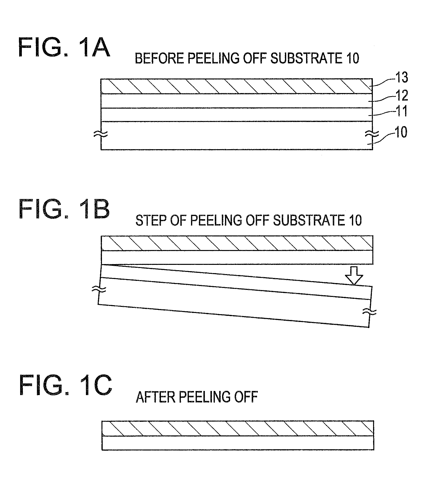
[0104]Hereinafter, a representative peeling off procedure utilizing the present invention will be schematically shown with reference to FIG. 1.

[0105]In FIG. 1A, the reference numeral 10 denotes a substrate, the reference numeral 11 denotes a nitride layer or a metal layer, the reference numeral 12 denotes an oxide layer, and the reference numeral 13 denotes a peeled off layer.

[0106]In FIG. 1A, as for the substrate 10, a glass substrate, a quartz substrate, a ceramic substrate or the like can be used. Moreover, a silicon substrate, a metal substrate or a stainless substrate may also be used.

[0107]First, as shown in FIG. 1A, the nitride layer or metal layer 11 is formed on the substrate 10. As the nitride layer or metal layer 11, representative examples are as follows: an element selected from Ti, Al, Ta, W, Mo, Cu, Cr, Nd, Fe, Ni, Co, Zr, Zn, Ru, Rh, Pd, Os, Ir and Pt, or a monolayer consisted of alloy materials or compound materials whose principal components are the foregoing eleme...

embodiment 2

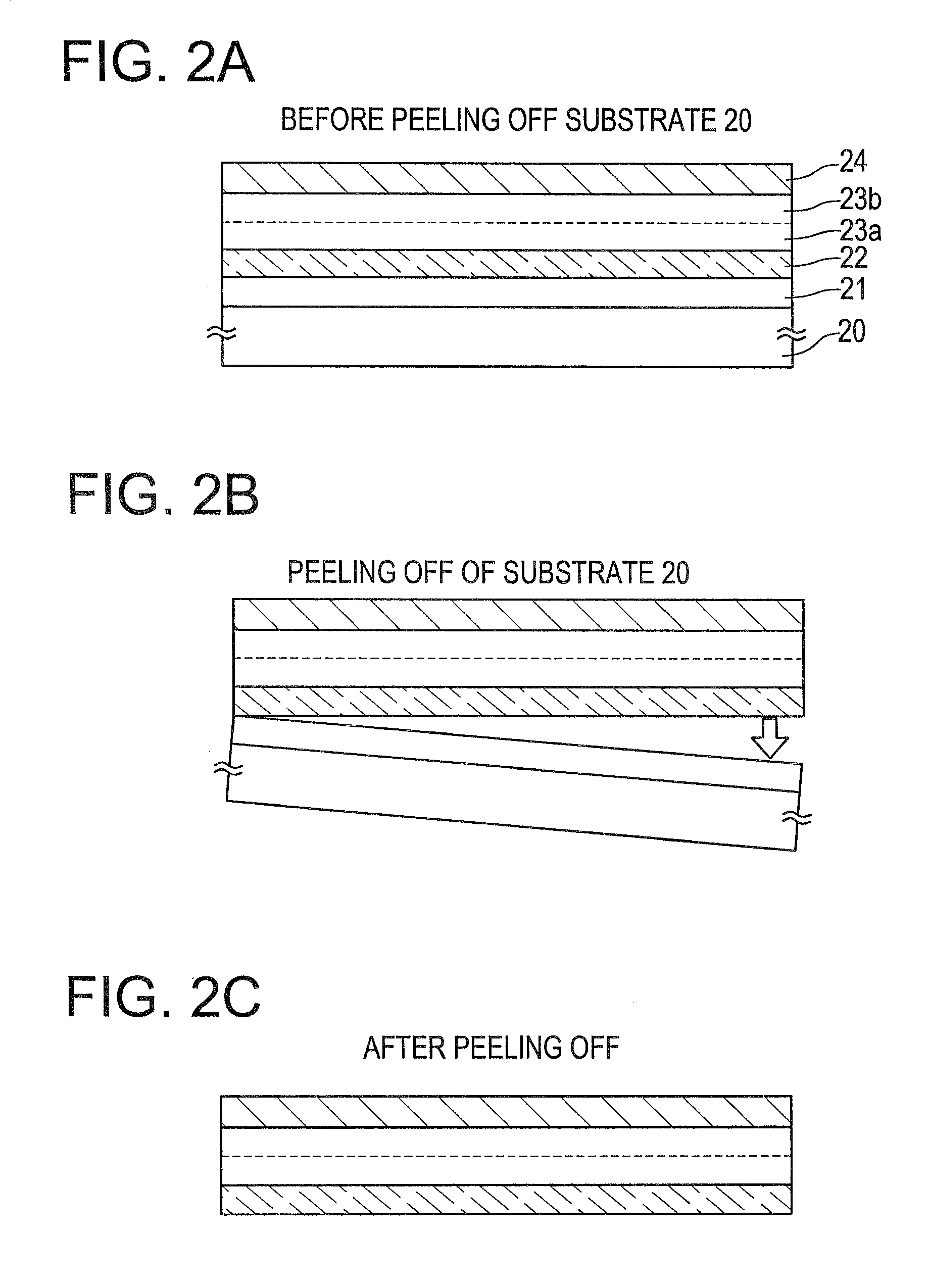
[0110]As for the present Embodiment, the peeling off procedure for peeling off the substrate while the impurities diffusion from the nitride layer or metal layer and the substrate is prevented by providing a primary coat insulating layer being in contact with the peeled off layer is schematically shown in FIG. 2. In FIG. 2 A, the reference numeral 20 denotes a substrate, the reference numeral 21 denotes a nitride layer or a metal layer, the reference numeral 22 denotes an oxide layer, the reference numerals and characters 23a and 23b denote primary coat insulating layers, and the reference numeral 24 denotes a peeled off layer.

[0111]In FIG. 2 A, as for the substrate 20, a glass substrate, a quartz substrate, a ceramic substrate or the like can be used. Moreover, a silicon substrate, a metal substrate or a stainless substrate may also be used.

[0112]First, as shown in FIG. 2 A, the nitride layer or metal layer 21 is formed on the substrate 20. As the nitride layer or metal layer 21, r...

embodiment 3

[0122]In the present embodiment, in addition to Embodiment 1, an example in which the irradiation of laser beam or the heat processing is performed in order to promote the peeling off is shown in FIG. 4.

[0123]In FIG. 4 A, the reference numeral 40 denotes a substrate, the reference numeral 41 denotes a nitride layer or a metal layer, the reference numeral 42 denotes an oxide layer and the reference numeral 43 denotes a peeled off layer.

[0124]Since the step of forming it until the peeled off layer 43 is made is the same with Embodiment 1, the description is omitted.

[0125]After the peeled off layer 43 was formed, the irradiation of laser beam is performed (FIG. 3 A). As a laser beam, a gas laser such as an excimer laser or the like, a solid state laser such as YVO4 laser, YAG laser or the like, and a semiconductor laser may be used. Moreover, the form of laser may be either of continuous oscillation or pulse oscillation, and the shape of the laser beam may be any of linear, rectangular...


PUM

PropertyMeasurementUnit
temperatureaaaaaaaaaa
thicknessaaaaaaaaaa
thicknessaaaaaaaaaa

Abstract

The present invention provides a peeling off method without giving damage to the peeled off layer, and aims at being capable of peeling off not only a peeled off layer having a small area but also a peeled off layer having a large area over the entire surface at excellent yield ratio. The metal layer or nitride layer 11 is provided on the substrate, and further, the oxide layer 12 being contact with the foregoing metal layer or nitride layer 11 is provided, and furthermore, if the lamination film formation or the heat processing of 500° C. or more in temperature is carried out, it can be easily and clearly separated in the layer or on the interface with the oxide layer 12 by the physical means.

Description

BACKGROUND OF THE INVENTION[0001]1. Field of the Invention[0002]The present invention relates to a method of peeling off a peeled off layer, particularly, relates to a method of peeling off a peeled off layer containing a variety of elements. In addition, the present invention relates to a semiconductor device having a circuit consisted of a thin film transistor (hereinafter, referred to as TFT) in which the peeled off layer peeled off has been pasted and transferred on a base member and a method of manufacturing the semiconductor device. For example, the present invention relates to an electro-optic device which is represented by a liquid crystal module, a light emitting device which is represented by an EL module and an electronic equipment on which such a device is mounted as a part.[0003]It should be noted that in the present specification, the term “semiconductor device” indicates a device in general capable of functioning by utilizing the semiconductor characteristics, and an ...

Claims


Application Information

Patent Timeline
Patent Type & Authority Patents(United States)
IPC IPC(8): H01L21/00H01L21/30H01L21/46H01L29/786G02F1/13357G02F1/1368G09F9/00G09F9/30H01L21/02H01L21/20H01L21/336H01L21/762H01L21/77H01L21/84H01L27/12H01L51/50H05B33/02H05B33/04H05B33/10
CPCH01L21/2007H01L21/76251H01L27/1214H01L27/1266H01L33/44G02F2001/13613H01L2924/0002H01L2227/326H01L2924/00H01L27/1218H01L27/1248G02F1/13613H10K71/80H10K59/1201H01L29/786H10K59/1213G02F1/1362H01L29/24H01L29/7869G02F1/1339G02F1/1341
Inventor TAKAYAMA, TORUMARUYAMA, JUNYAMIZUKAMI, MAYUMIYAMAZAKI, SHUNPEI
Owner SEMICON ENERGY LAB CO LTD
Why Eureka
Try Eureka