

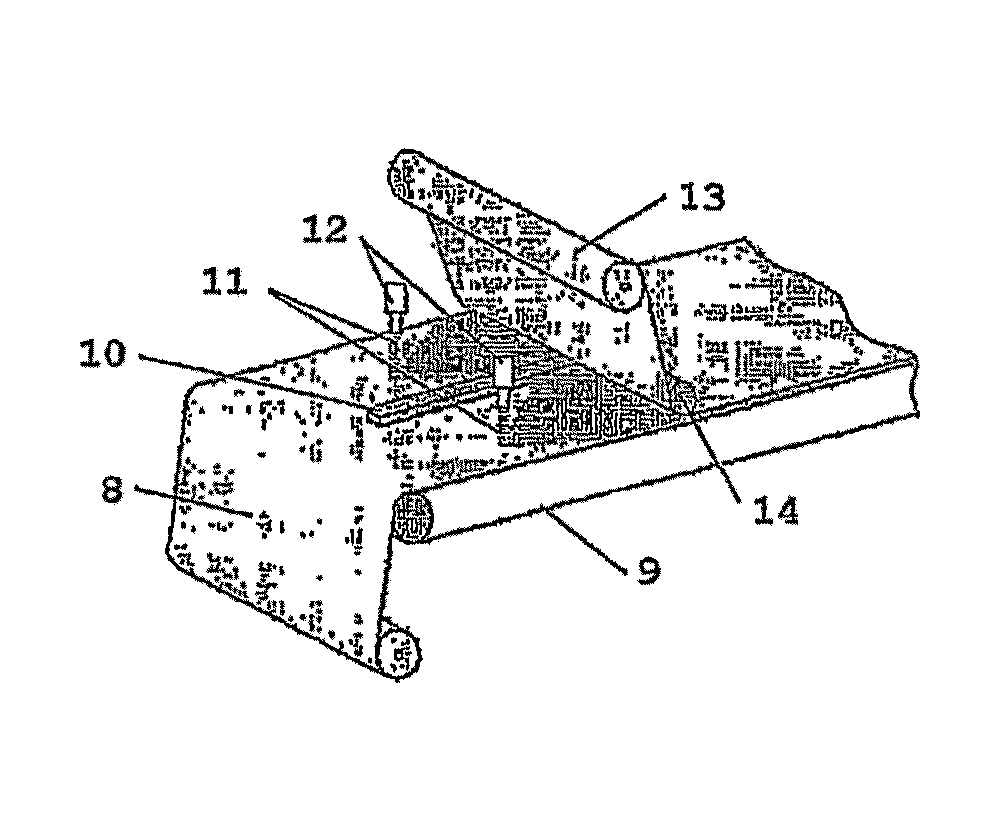
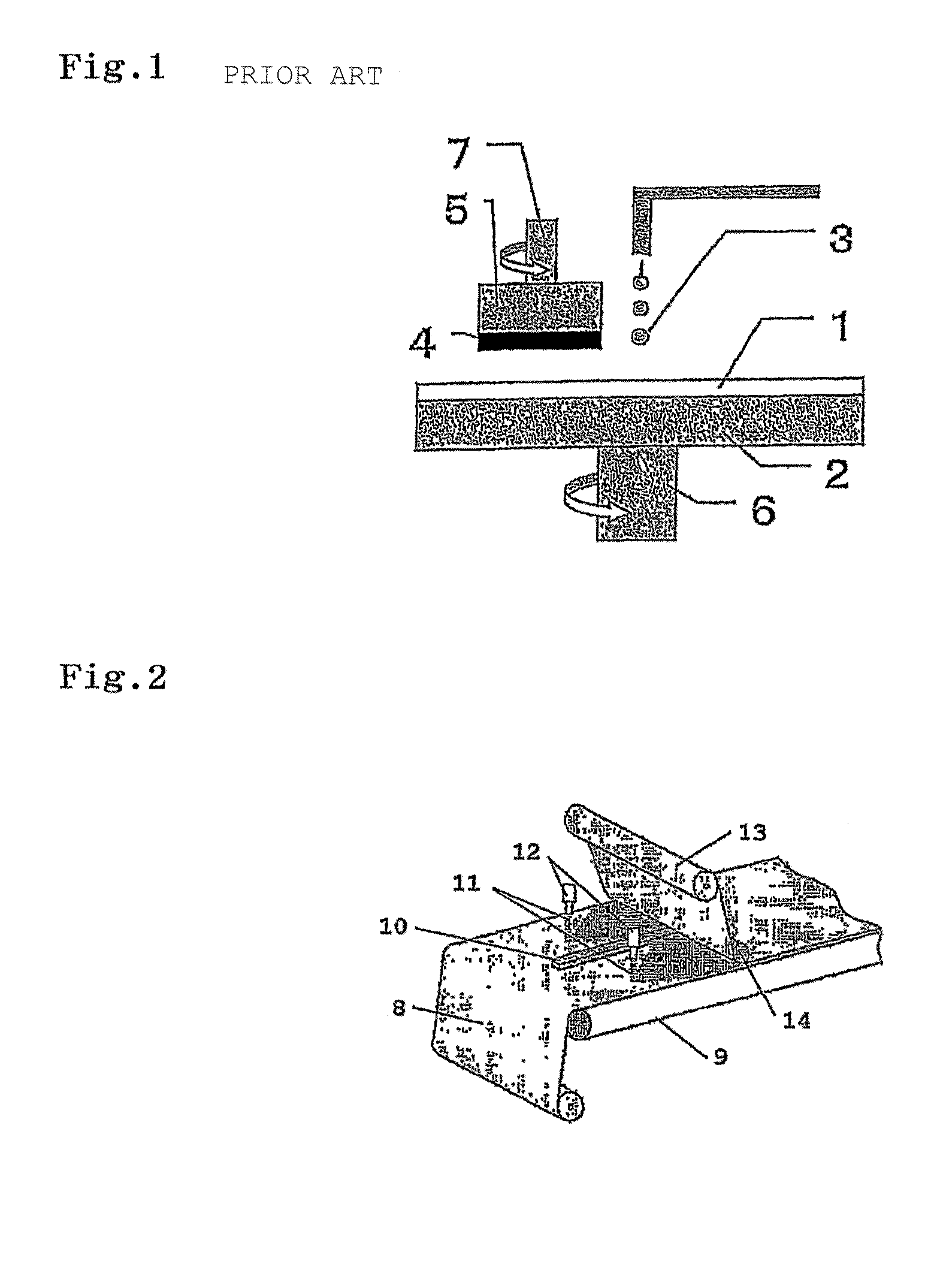
Process for manufacturing polishing pad
a polishing pad and manufacturing technology, applied in the direction of manufacturing tools, grinding devices, transportation and packaging, etc., can solve the problems of judging the planarity of the surface waste of treatment time of the test wafer and the cost of treatment, and difficult to accurately predict the processing results without actual processing of the product, etc., to achieve long polishing pads, high light transmittance and flexibility, and high productivity
- Summary
- Abstract
- Description
- Claims
- Application Information
AI Technical Summary
Benefits of technology
Problems solved by technology
Method used
Image

Examples
examples
[0099]Description will be given of the invention with examples, while the invention is not limited to description in the examples.
[0100]Measurement of Asker D Hardness
[0101]The measurement was performed according to JIS K6253-1997. Pieces of a size of 2 cm×2 cm (arbitrarily thick) cut from the light-transmitting region were used as hardness measurement samples. A water-impermeable film was produced from each of the polyurethane resin coating compositions used in Examples 1 and 2 and Comparative Example 1 and then cut into pieces of a size of 2 cm×2 cm (arbitrarily thick), which were also used as hardness measurement samples. The PET substrate used in Comparative Example 2 was cut into pieces of a size of 2 cm×2 cm (arbitrarily thick), which were also used as hardness measurement samples. These hardness measurement samples were allowed to stand in an environment at a temperature of 23° C.±2° C. and a humidity of 50%±5% for 16 hours. An at least 6 mm-thick laminate of each type of sam...
example 1
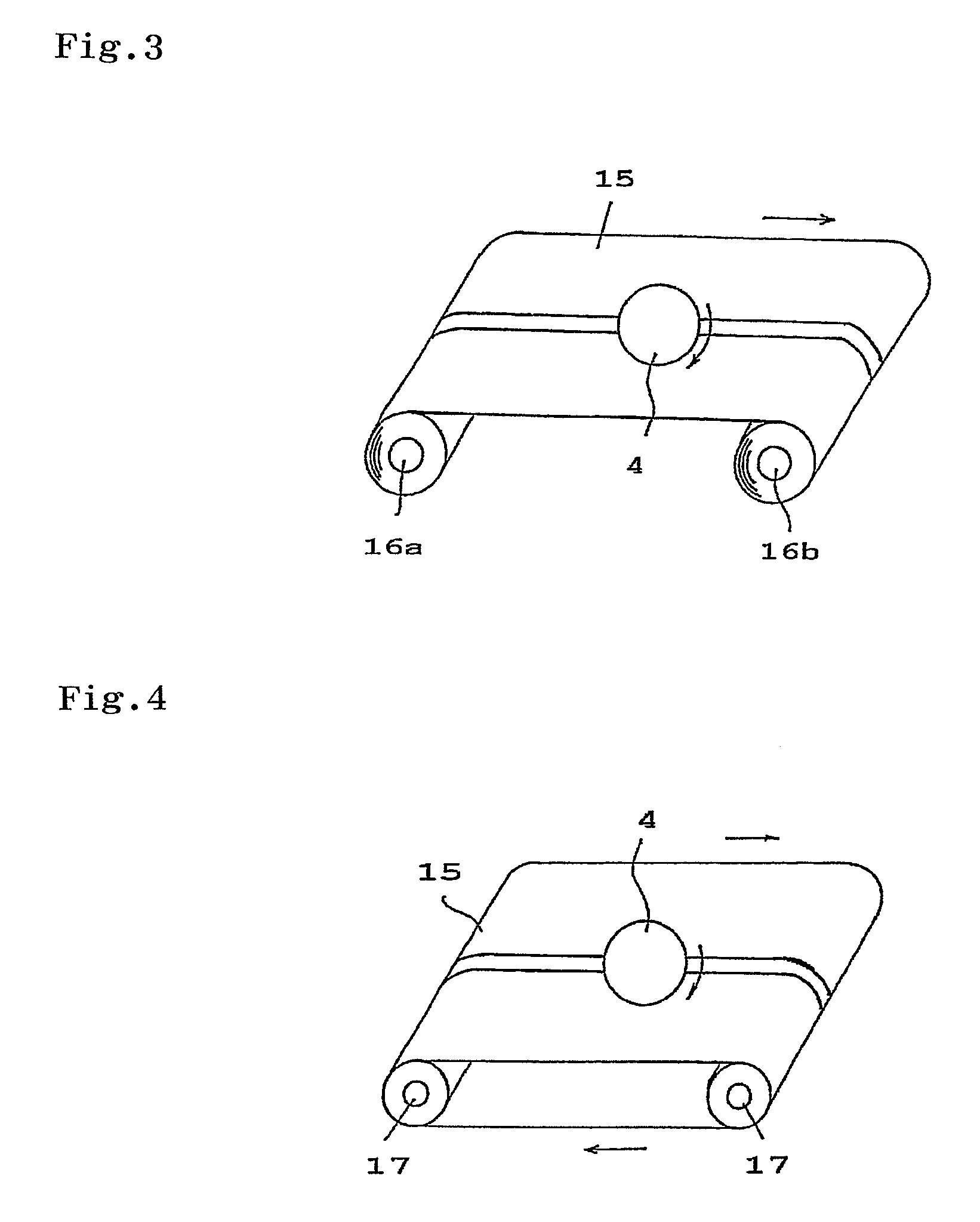
[0119]A liquid mixture was obtained by mixing and stirring 7 parts by weight of 1,4-butanediol, 7 parts by weight of trimethylolpropane, 21.1 parts by weight of polytetramethylene glycol with a number average molecular weight of 650, and 0.6 parts by weight of a catalyst (Kao No. 25, manufactured by Kao Corporation). 100 parts by weight of an HDI prepolymer (Coronate 2612, manufactured by Nippon Polyurethane Industry Co., Ltd.) was added to the liquid mixture. The mixture was thoroughly stirred using a hybrid mixer and then degassed, so that a polyurethane resin coating composition was prepared. The polyurethane resin coating composition was applied to the whole of the back surface of the prepared long polishing sheet and cured by heating at 70° C. to form a water-impermeable film (20 μm in thickness, 20 degrees in D hardness), so that a long polishing pad was obtained.
example 2
[0120]A liquid mixture was obtained by mixing and stirring 12.6 parts by weight of 1,4-butanediol, 3.4 parts by weight of trimethylolpropane, 6.9 parts by weight of polytetramethylene glycol with a number average molecular weight of 650, and 0.6 parts by weight of a catalyst (Kao No. 25, manufactured by Kao Corporation). 100 parts by weight of an HDI prepolymer (Coronate 2612, manufactured by Nippon Polyurethane Industry Co., Ltd.) was added to the liquid mixture. The mixture was thoroughly stirred using a hybrid mixer and then degassed, so that a polyurethane resin coating composition was prepared. The polyurethane resin coating composition was applied to the whole of the back surface of the prepared long polishing sheet and cured by heating at 70° C. to form a water-impermeable film (40 μm in thickness, 39 degrees in D hardness), so that a long polishing pad was obtained.
PUM
| Property | Measurement | Unit |
|---|---|---|
| thickness | aaaaa | aaaaa |
| particle sizes | aaaaa | aaaaa |
| wavelengths | aaaaa | aaaaa |
Abstract
Description
Claims
Application Information