Organic electroluminescence element

a technology of electroluminescence elements and organic materials, applied in the field of organic electroluminescence elements, can solve the problems of instability of elements, deterioration of luminescence efficiency, rise of drive voltage, etc., and achieve the effect of high transparency

Inactive Publication Date: 2013-05-21
JOLED INC +1
View PDF24 Cites 9 Cited by
  • Summary
  • Abstract
  • Description
  • Claims
  • Application Information

AI Technical Summary

Benefits of technology

[0023]Furthermore, although the fullerenes described in Patent Reference 3 have high damage resistance against sputter, plasma, and the like, when the fullerenes come directly into contact with the organic luminescent layer, there is an energy transfer of the luminescence exciton energy generated within the organic luminescent layer during driving of the organic EL, to the fullerene layer, and thus luminescence efficiency deteriorates. In other words, there is the problem that the fullerenes cause optical-quenching of the luminescence of the organic luminescent layer, which greatly reduces the luminescence efficiency of the element.
[0044]With the organic EL element of the present invention, electron injection from the transparent cathode to the luminescent layer is promoted, the luminescent layer is protected from damage during forming of the transparent cathode, and the electron injecting function and electron transporting function with high transparency is ensured, and thus it is possible to provide an organic EL element having a transparent cathode as a top electrode, and excelling in all of luminescence efficiency, drive voltage, and operational life.

Problems solved by technology

However, with the π (pi) electron low-molecular-weight electron transport material described in Patent Reference 2, damage from sputter damage is significant and, although damage to the organic luminescent layer is reduced, there is the problem that the layer of the electron transport material itself is damaged, leading to the instability of the element, the rise of drive voltage, and so on.
Furthermore, although the fullerenes described in Patent Reference 3 have high damage resistance against sputter, plasma, and the like, when the fullerenes come directly into contact with the organic luminescent layer, there is an energy transfer of the luminescence exciton energy generated within the organic luminescent layer during driving of the organic EL, to the fullerene layer, and thus luminescence efficiency deteriorates.
In other words, there is the problem that the fullerenes cause optical-quenching of the luminescence of the organic luminescent layer, which greatly reduces the luminescence efficiency of the element.
Furthermore, the alkaline fluoride described in Patent Reference 4 is oxidized by the cathode of a transparent oxide such as ITO, used as the upper electrode including a conductive material, and there is a problem that the stability and operational life of the organic EL element significantly deteriorates.
Furthermore, in the case where a fullerene layer is laminated in the upper layer of the layer including alkaline fluoride, there is the problem that alkaline fluoride is not sufficiently reduced to the metal state required for implementing electron injection, and good electron injection to the organic luminescent layer cannot be obtained.

Method used


Image

  • Organic electroluminescence element
  • Organic electroluminescence element
  • Organic electroluminescence element

Examples


example 1

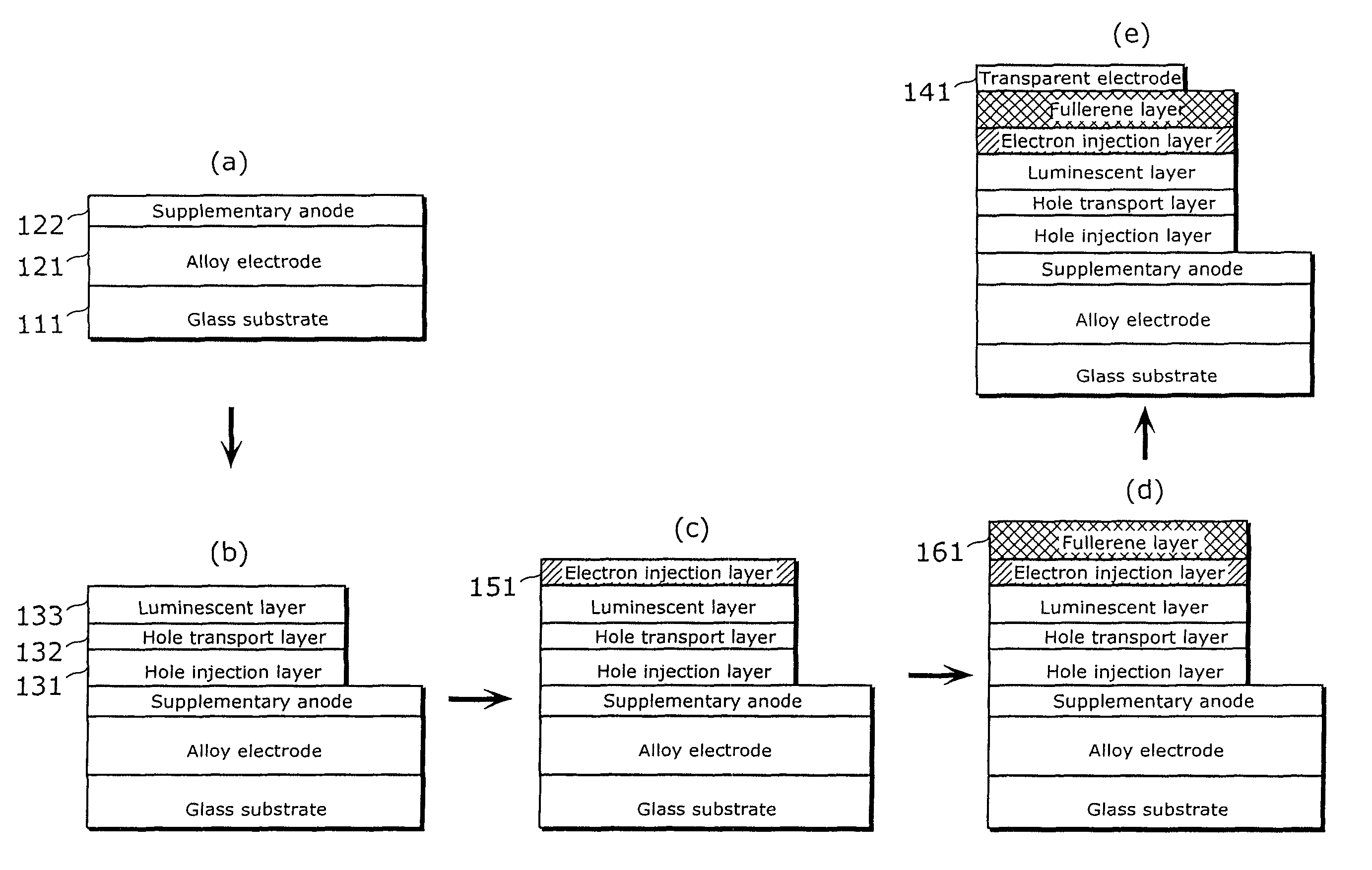
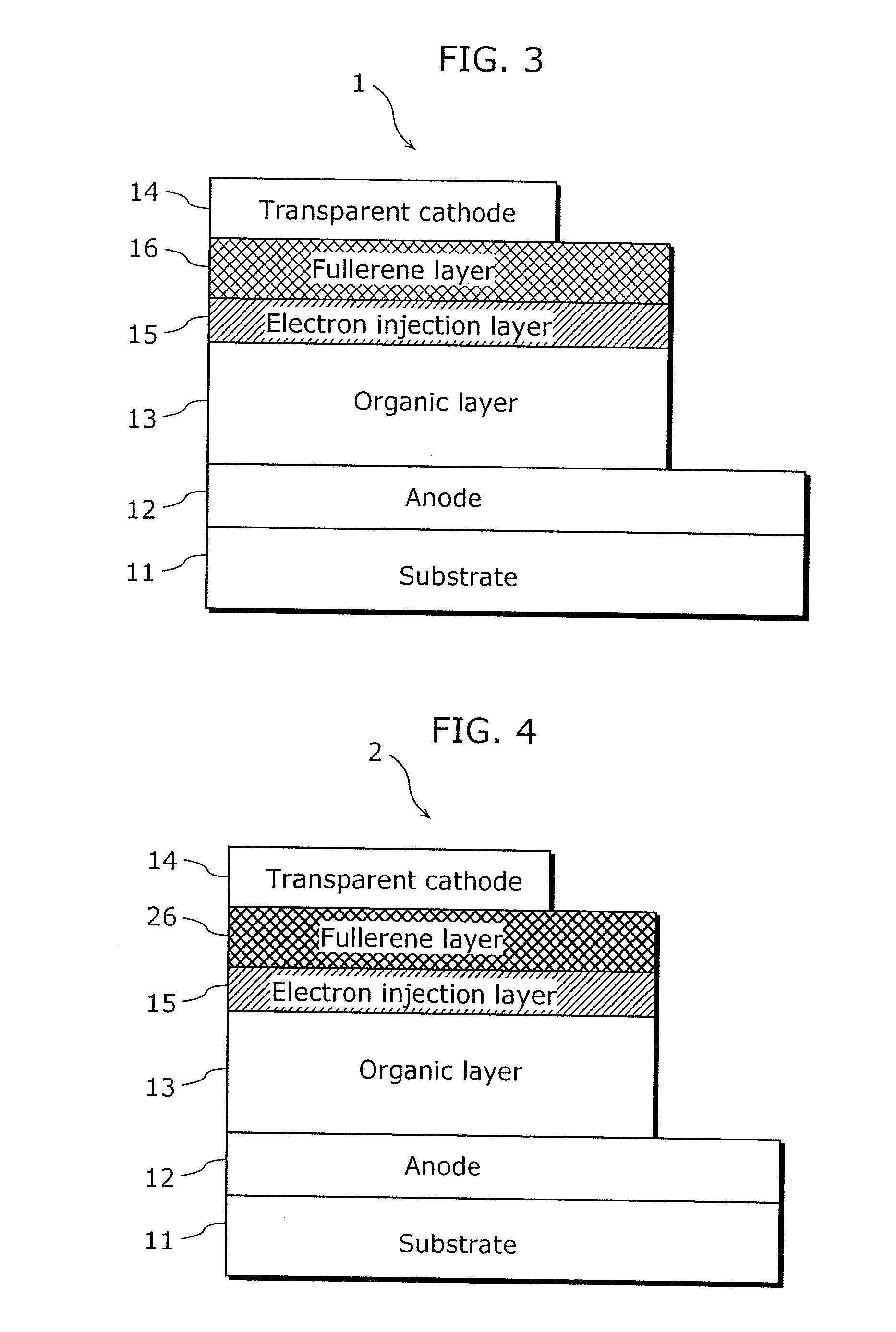
[0077]FIG. 5 is a process diagram describing the manufacturing method for the organic EL element in example 1 of the present invention. First, a 100-nm-thick, 97% molybdenum and 3% chrome alloy electrode 121 was formed on the surface of a glass substrate 111 (using flat glass manufactured by Matsunami Glass Ind. Ltd.) by sputtering. Then, the alloy electrode 121 was patterned into the anode shape by photolithography. Next, as a supplementary anode 122, a 60-nm-thick indium tin oxide electrode was formed on the surface of the patterned alloy electrode 121 by sputtering, and patterned into a predetermined anode shape by photolithography (FIG. 5(a)). The patterned alloy electrode 121 and supplementary anode 122 each have the function of an anode.

[0078]Next, the following three layers were formed as the organic layer. First, a 60-nm-thick hole injection layer 131 was formed by forming polyethylenedioxythiophene (PEDOT: Baytron P AI 4083 manufactured by TA Chemical Co.) on the surface of...

example 2

[0082]In the manufacturing method for the organic EL element in example 2 of the present invention, the organic EL element was formed in the same manner as in example 1 except that the fullerene layer was formed by changing the thickness of the fullerene layer 161 described in FIG. 5, from 10 nm to 20 nm.

example 3

[0083]In the manufacturing method for the organic EL element in example 3 of the present invention, the organic EL element was formed in the same manner as in example 1 except that the fullerene layer was formed by changing the thickness of the fullerene layer 161 described in FIG. 5, from 10 nm to 50 nm.


PUM

PropertyMeasurementUnit
thicknessaaaaaaaaaa
thicknessaaaaaaaaaa
thicknessaaaaaaaaaa

Abstract

An organic electroluminescence element having a cathode as a top electrode, and excelling in luminance efficiency, drive voltage, and operational life is provided. The organic electroluminescence element includes an anode over a substrate and a luminescent layer over the anode. The luminescent layer comprises an organic material. An electron injection layer is over the luminescent layer for injecting electrons into the luminescent layer. The electron injection layer is a metal including at least one of an alkaline metal and an alkaline earth metal. A fullerene layer is over the electron injection layer and includes fullerenes and at least one of an alkaline metal and an alkaline earth metal. The at least one of the alkaline metal and the alkaline earth metal included in the fullerene layer has a lower work function than a lowest unoccupied molecular orbit energy level of the fullerenes. A cathode is over the fullerene layer.

Description

CROSS REFERENCE TO RELATED APPLICATION(S)[0001]This is a continuation application of PCT Application No. PCT / JP2009 / 002347 filed May 27, 2009, designating the United States of America, the disclosure of which, including the specification, drawings, and claims, is incorporated herein by reference in its entirety.[0002]The disclosure of United Kingdom Patent Application No. 0810044.8 filed on Jun. 2, 2008, including the specification, drawings and claims, is incorporated herein by reference in its entirety.BACKGROUND OF THE INVENTION[0003]1. Field of the Invention[0004]The present invention relates to organic electroluminescence elements, and particularly to an organic electroluminescence element used in display devices and lighting, and manufacturing method thereof.[0005]2. Description of the Related Art[0006]An element from which luminescence (electroluminescence) can be obtained by applying voltage to a thin film of organic material sandwiched between two electrodes is called an or...

Claims


Application Information

Patent Timeline
Patent Type & Authority Patents(United States)
IPC IPC(8): H01L29/08H01L51/00H01L35/24
CPCB82Y10/00H01L51/0048H01L51/5234H05B33/10H05B33/14H10K85/221H10K59/80524H05B33/02H10K50/171H10K50/828
Inventor OKUMOTO, KENJIBURROUGHES, JEREMYCARTER, JULIAN
Owner JOLED INC
Why Eureka
Try Eureka