

Latent electrostatic image bearing member, and image forming apparatus, image forming method and process cartridge using the same
a technology of electrostatic image bearing and image forming process, which is applied in the direction of corona discharge, instruments, photosensitive materials, etc., can solve the problems of poor failure to conduct the proper image formation process, and change in electrical characteristics of photoconductor, etc., to achieve excellent electrographic characteristics, stable image formation, and high wear resistance
- Summary
- Abstract
- Description
- Claims
- Application Information
AI Technical Summary
Benefits of technology
Problems solved by technology
Method used
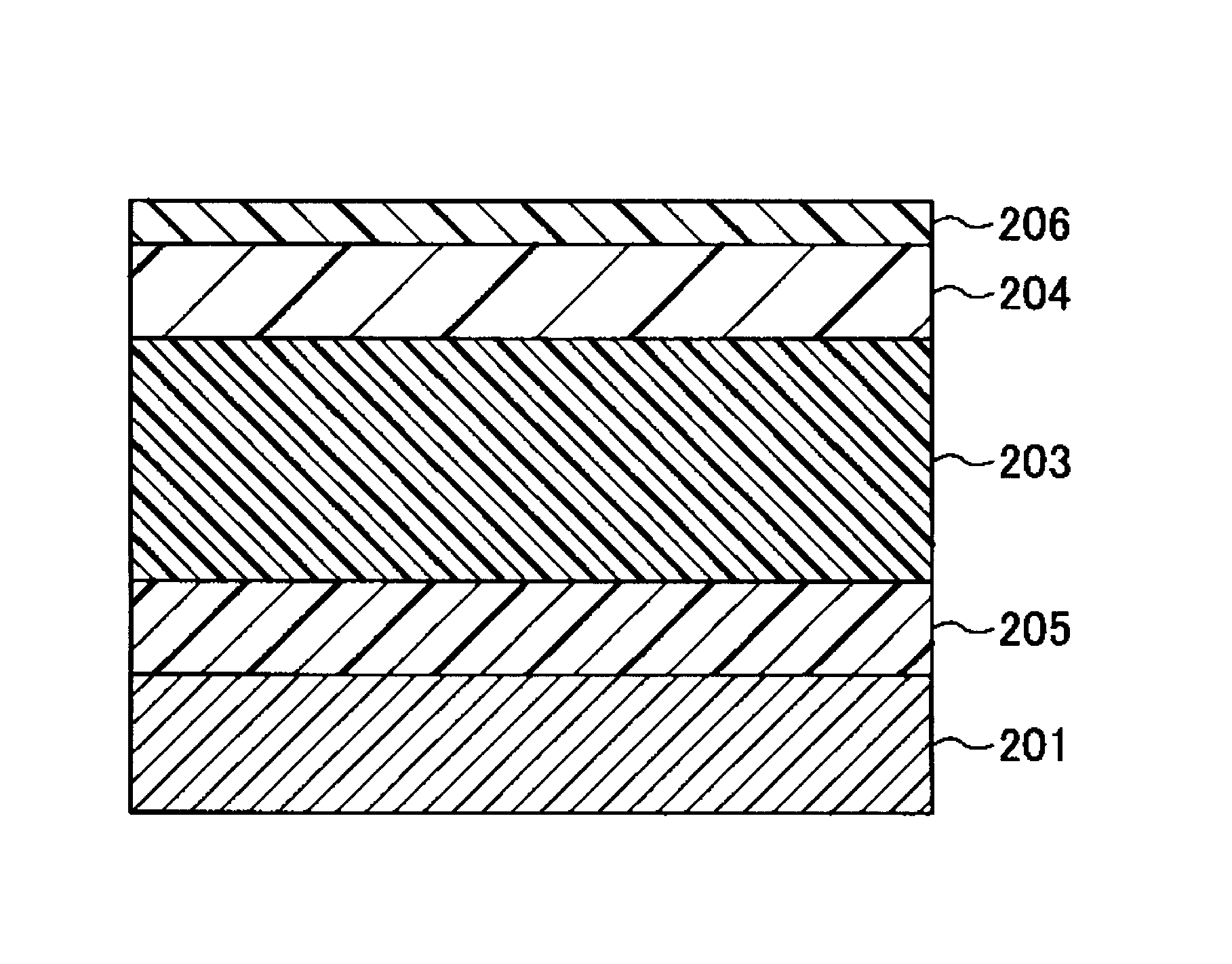
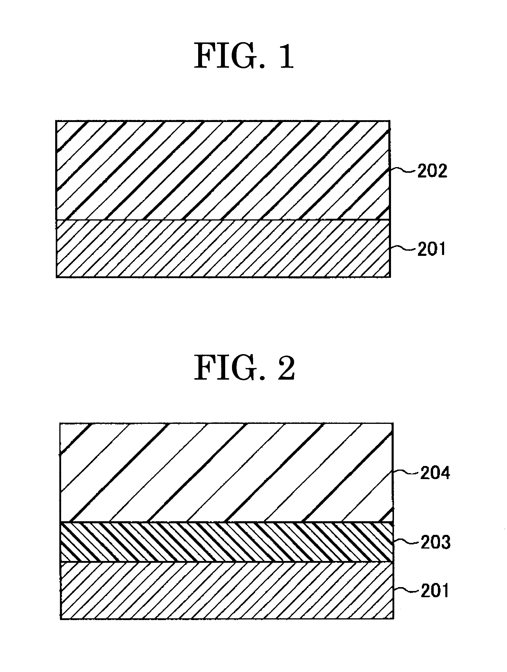
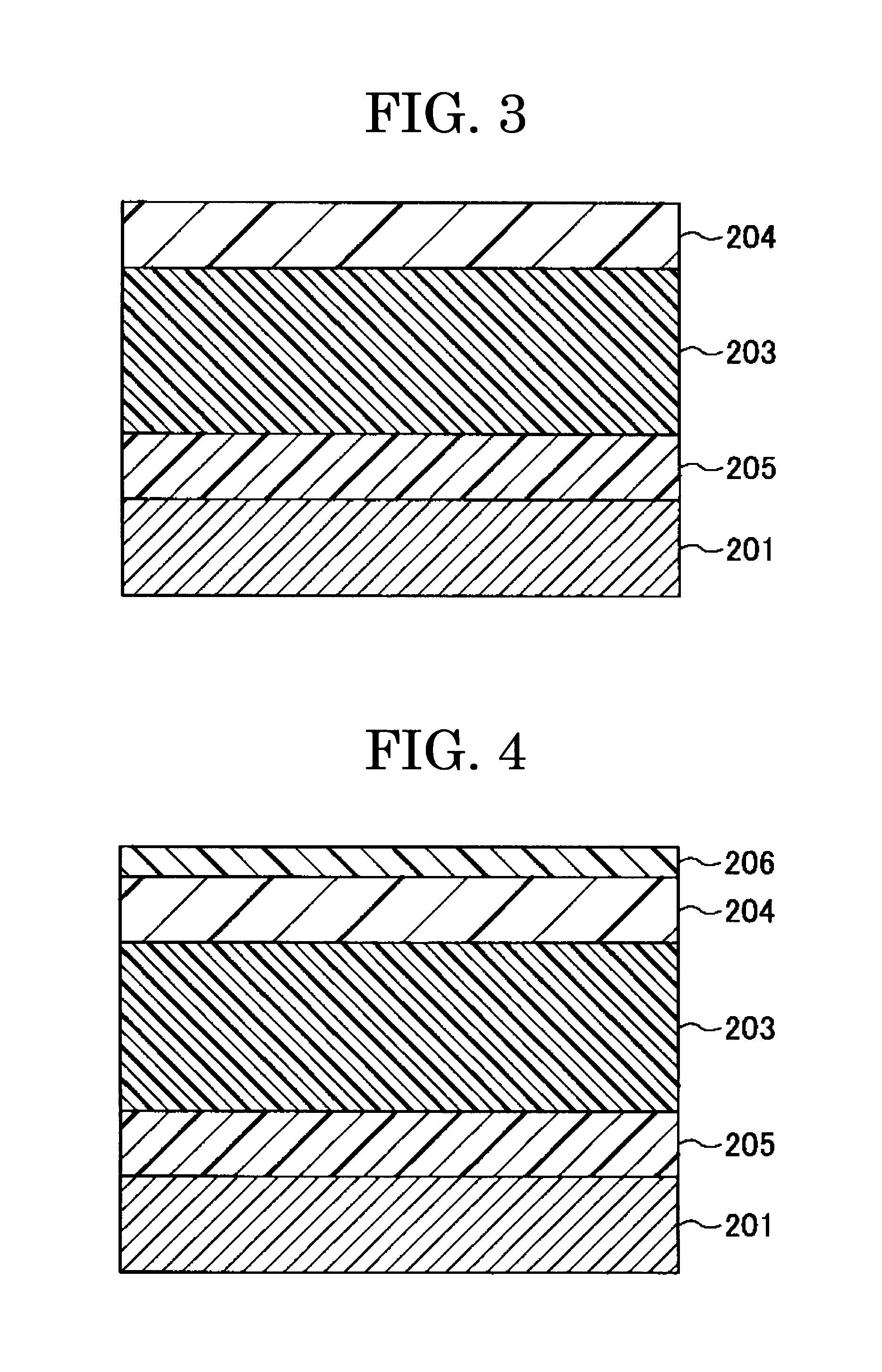
Image

Examples
preparation example 1
[0532]A reaction vessel equipped with a condenser tube, stirrer and nitrogen feed tube was charged with 724 parts of bisphenol A ethylene oxide (2 mol) adduct, 276 parts of isophthalic acid, and 2 parts of dibutyltin oxide, allowing reaction to proceed at 230° C. for 8 hours under normal pressure, and then under reduced pressure of 10-15 mmHg for 5 hours, and the vessel was cooled to 160° C. The reaction vessel was then charged with 32 parts of phthalic anhydride for reaction for a further 2 hours. The vessel was cooled to 80° C. and the resultant product was reacted with 188 parts of isophorone diisocyanate for 2 hours in ethyl acetate to give an isocyanate containing-prepolymer (1), 267 parts of which was then reacted with 14 parts of isophorone diamine for 2 hours at 50° C. to give a urea-modified polyester resin (1) with a weight-average molecular weight of 6,4000. In a similar way 724 parts of bisphenol A ethylene oxide (2 mol) adduct was condensed with 276 parts of terephthali...
preparation example 2
[0537]In 2,000 parts of a 1:1 mixture solvent of ethyl acetate and MEK were dissolved 850 parts of the urea-modified polyester resin (1) and 150 parts of the unmodified polyester resin (a), both prepared in Preparation Example 1, to give a toner binder resin (2) in ethyl acetate / MEK solution. A portion of this solution was dried under reduced pressure to isolate toner binder resin (2). The toner of Preparation Example 2 was prepared in the same manner as that of Preparation Example 1 except that the toner binder resin (2) was employed instead of the toner binder resin (1). The average circularity of this toner, measured as in Preparation Example 1, was 0987.
preparation example 3
[0538]A reaction vessel equipped with a condenser tube, stirrer and nitrogen feed tube was charged with 343 parts of bisphenol A ethylene oxide (2 mol) adduct, 166 parts of isophthalic acid, and 2 parts of dibutyltin oxide, allowing reaction to proceed at 230° C. for 8 hours under normal pressure, and then under reduced pressure of 10-15 mmHg for 5 hours, and the vessel was cooled to 80° C. The resultant product was reacted with 14 parts of toluene diisocyanate in toluene at 110° C. for 5 hours. After the reaction completed, solvent removal was conducted to give a urethane-modified polyester resin with a weight-average molecular weight of 98,000.
[0539]As in Preparation Example 1, 363 parts of bisphenol A ethylene oxide (2 mol) adduct was condensed with 166 parts of terephthalic acid at 230° C. to give a unmodified polyester resin.
[0540]In toluene 350 parts of the urethane-modified polyester resin and 650 parts of the unmodified polyester resin were dissolved and mixed, and toluene w...
PUM
| Property | Measurement | Unit |
|---|---|---|
| particle diameter | aaaaa | aaaaa |
| volume-average particle diameter | aaaaa | aaaaa |
| thickness | aaaaa | aaaaa |
Abstract
Description
Claims
Application Information