Magneto-impedance sensor element and method for manufacturing the same
a technology of magnetic sensor and magnetic element, which is applied in the field of magnetic sensor element and method for manufacturing the same, can solve the problems of insufficient high-performance magnetic sensor, insufficient stress-free amorphous wire, and insufficient exertion of mi effect, so as to prevent the formation of extending grooves and reduce the thickness of the substrate. , the effect of sufficient strength
- Summary
- Abstract
- Description
- Claims
- Application Information
AI Technical Summary
Benefits of technology
Problems solved by technology
Method used
Image
Examples
embodiments
Embodiment 1
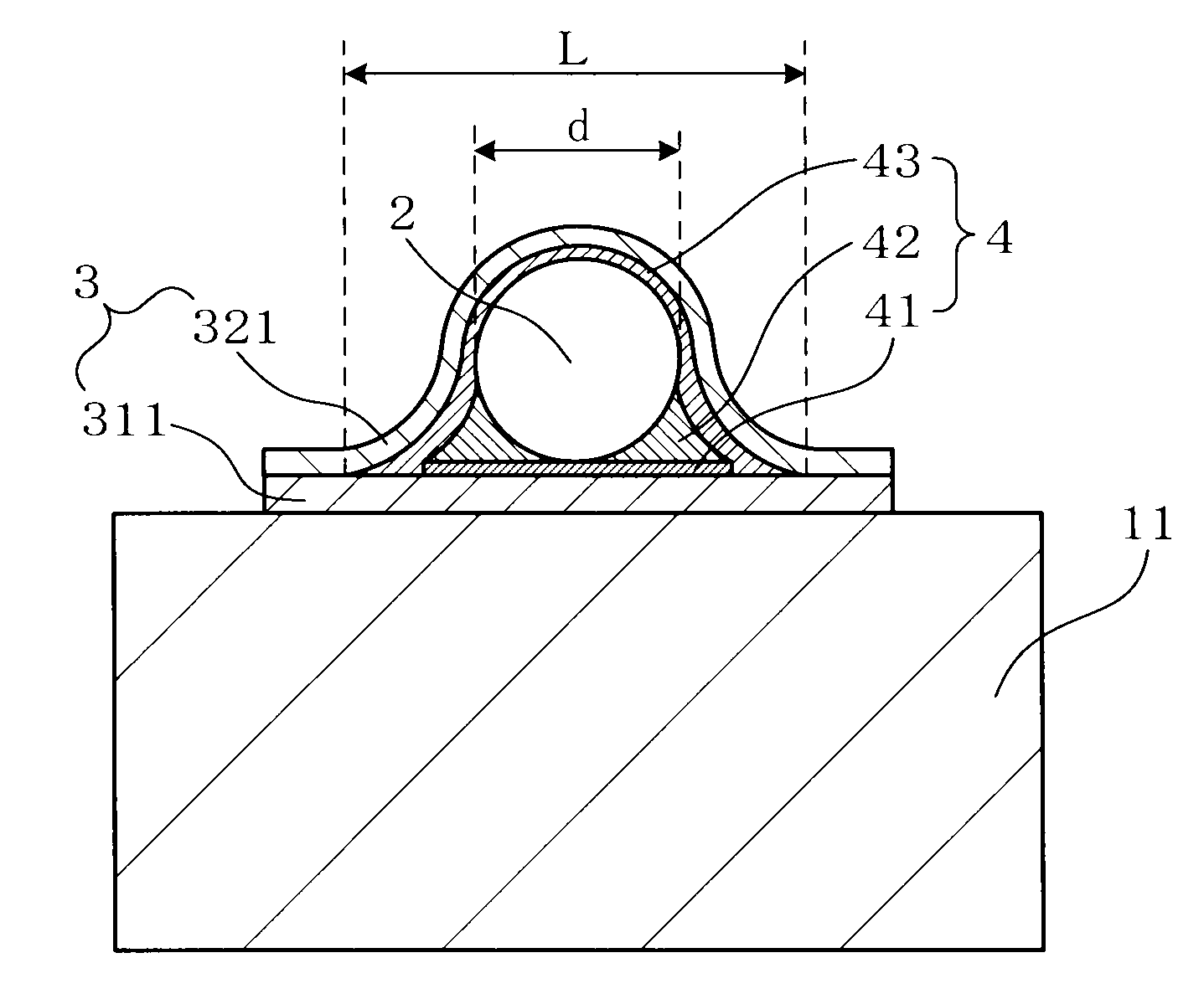
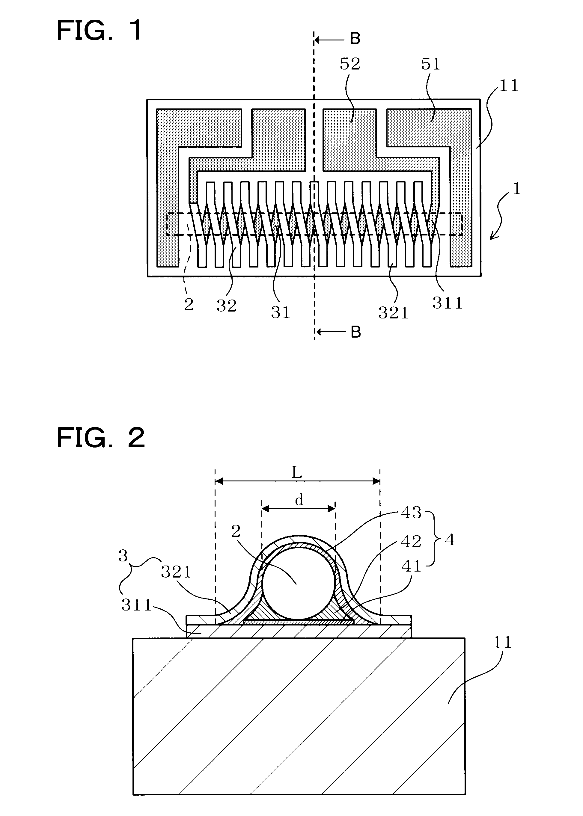
[0130]A first embodiment of a planar type MI element according to the present invention will be described below with reference to FIGS. 1 and 2. FIG. 1 is a conceptual diagram showing a front side of a planar type MI element 1, and FIG. 2 is a view on arrow along a B-B line in FIG. 1.
[0131]As shown in FIGS. 1 and 2, the magneto-impedance sensor element 1 according to the present invention includes a substrate 11 formed of a nonmagnetic material. The magneto-impedance sensor element 1 includes a planar pattern 31 configured by a plurality of first conductive films 311 arranged on a flat surface of a substrate surface. The magneto-impedance sensor element 1 includes an amorphous wire 2 having a circular section that is arranged along an aligning direction of the planar pattern 31 so as to traverse the plurality of first conductive films 311. Furthermore, the magneto-impedance sensor element 1 includes an insulator 4 that covers an outer peripheral surface of the amorphous ...
embodiment 2
[0176]In Embodiment 2, the same material as that of the amorphous wire in Embodiment 1 and the conventional technique is used, a wire diameter is reduced from 30 μm to 10 μm, and a wire length is shortened from 0.9 mm to 0.57 mm. Accordingly, the length of the substrate is shortened from 1.0 mm to 0.6 mm. The other conditions are the same as those in Embodiment 1.
[0177]As a result, a diameter of a substantial circle of a detecting coil in Embodiment 2 can be considerably reduced in size to about 19 μm in comparison with about 43 μm in Embodiment 1 and the entire substrate height can be more reduced. The proximity index n given by (diameter of substantial circle of detecting coil) / (amorphous wire diameter) was 1.9 in Embodiment 2. Although inferior to Embodiment 1, a proximate winding is achieved in Embodiment 2 in comparison with the conventional technique in which n=2.2.
[0178]Furthermore, L / d=2.8 can be obtained. The value falls within the range of 1.3 to 5.
[0179]A sensitivity of t...
embodiment 3
[0185]The embodiment is obtained by changing the configuration of the insulator 4. As shown in FIG. 5, in this embodiment, the planar insulating portion 41 is formed simultaneously and integrally with the wire fixing portion 42.
[0186]In this case, since the step of forming the planar insulating portion 41 can be omitted, the steps in manufacturing the magneto-impedance sensor element 1 are simplified.
PUM
 Abstract
Description
Claims
Application Information


