Display device

a technology of a display device and a display screen, which is applied in the direction of discharge tube luminescnet screens, instruments, and semiconductor/solid-state device details, etc., can solve the problems of signal delay and electrical power loss, low adhesiveness of glass substrates, and large wiring resistance, and achieve excellent adhesiveness and low electrical resistivity. , the effect of high adhesiveness

Active Publication Date: 2013-07-09
KOBE STEEL LTD
View PDF60 Cites 24 Cited by
  • Summary
  • Abstract
  • Description
  • Claims
  • Application Information

AI Technical Summary

Benefits of technology

[0022]A display device according to the present invention is provided with a Cu alloy film (wiring film) having the multilayer structure, which includes a first layer (Y) composed of a Cu alloy containing predetermined elements excellent in the adhesiveness to a transparent substrate and a second layer (X) composed of pure Cu or a Cu alloy having an electrical resistivity lower than that of the first layer (Y), and hence both the high adhesiveness to the transparent substrate and a low electrical resistivity as the whole Cu alloy film can be achieved. With respect to the adhesiveness, still better adhesiveness can be achieved by appropriately controlling the thickness of the first layer (Y) and the content of Mn in the first layer (Y), in addition to the fact that the alloy element in the first layer (Y) is particularly made to be Mn. Further, in particular, the Cu alloy film employed in the present invention is extremely excellent in the resistance for the migration of sodium ion, etc., (migration resistance), which may occur when an inexpensive soda-lime glass substrate is used, and hence the Cu alloy film can be used in an extremely suitable manner as a wiring material for the display device provided with a soda-lime glass substrate. Furthermore, the Cu alloy film employed in the invention has the multilayer structure including similar pure Cu or Cu alloys, which does not cause an extreme difference in the etching rate between them, and hence fine-processing excellent in forming a shape, by which a pattern can be easily formed, can be performed by using the aforementioned Cu alloy film.

Problems solved by technology

However, with the growth in size and the high definition of the display devices, problems resulting from a fact that a wiring resistance is large, such as signal delay and electrical power loss, are coming to the surface.
However, Cu has the problem that the adhesiveness thereof to a glass substrate is low, and may be peeled off.
In particular, in the case of a soda-lime glass substrate (glass substrate comprising silicic acid, soda ash, and lime as the main materials) that is inexpensive and capable of being processed to have a large area, peel off of a wiring material, occurring due to the migration of alkali metal elements contained in the glass substrate, such as Na, becomes a problem.
Also, there is the problem that, because the adhesiveness of Cu to a glass substrate is low, it is difficult to perform wet etching for processing Cu into a wiring shape.
In these techniques, however, a process for forming the layer composed of a metal having high meting temperature becomes further necessary, and accordingly the manufacturing cost of a display device is increased.
In addition, because dissimilar metals of Cu and a metal (Mo, or the like) having high melting temperature are laminated one on another, there is the fear that corrosion may occur on the interface between Cu and the metal having high melting temperature when wet etching is performed.
Further, because there is a difference in the etching rate between the dissimilar metals, the problem that the wiring section cannot be formed into a desired shape (e.g., a shape having a taper angle of approximately 45 to 60°) may arise.
Furthermore, because the electrical resistivity of a metal having high melting temperature, for example, that of Cr (12.9×10⁻⁶ Ω*cm), is higher than that of Cu, and accordingly a signal delay or electrical power loss, occurring due to the wiring resistance, becomes a problem.
In the technique, however, the resin film is deteriorated in the high-temperature annealing process during the manufacture of a display device (e.g., liquid crystal panel), and accordingly there is the fear that the adhesiveness thereof may be decreased.
However, copper nitride itself is not a stable compound.
Accordingly, in the technique, N atoms are released as N2 gas in the high-temperature annealing process during the manufacture of a display device (e.g., liquid crystal panel), resulting in the deterioration of the wiring film, and accordingly there is the fear that the adhesiveness thereof may be decreased.

Method used


Image

  • Display device
  • Display device
  • Display device

Examples


example 1

Production of Samples

[0095]In the present example, with respect to the samples (Nos. 3 to 35) shown in Table 1 produced in the following way, influences on the electrical resistivity and the adhesiveness to the glass substrate by the type and content of the Cu alloy of which the first layer (Y) was composed and by the thickness of the first layer (Y) were investigated.

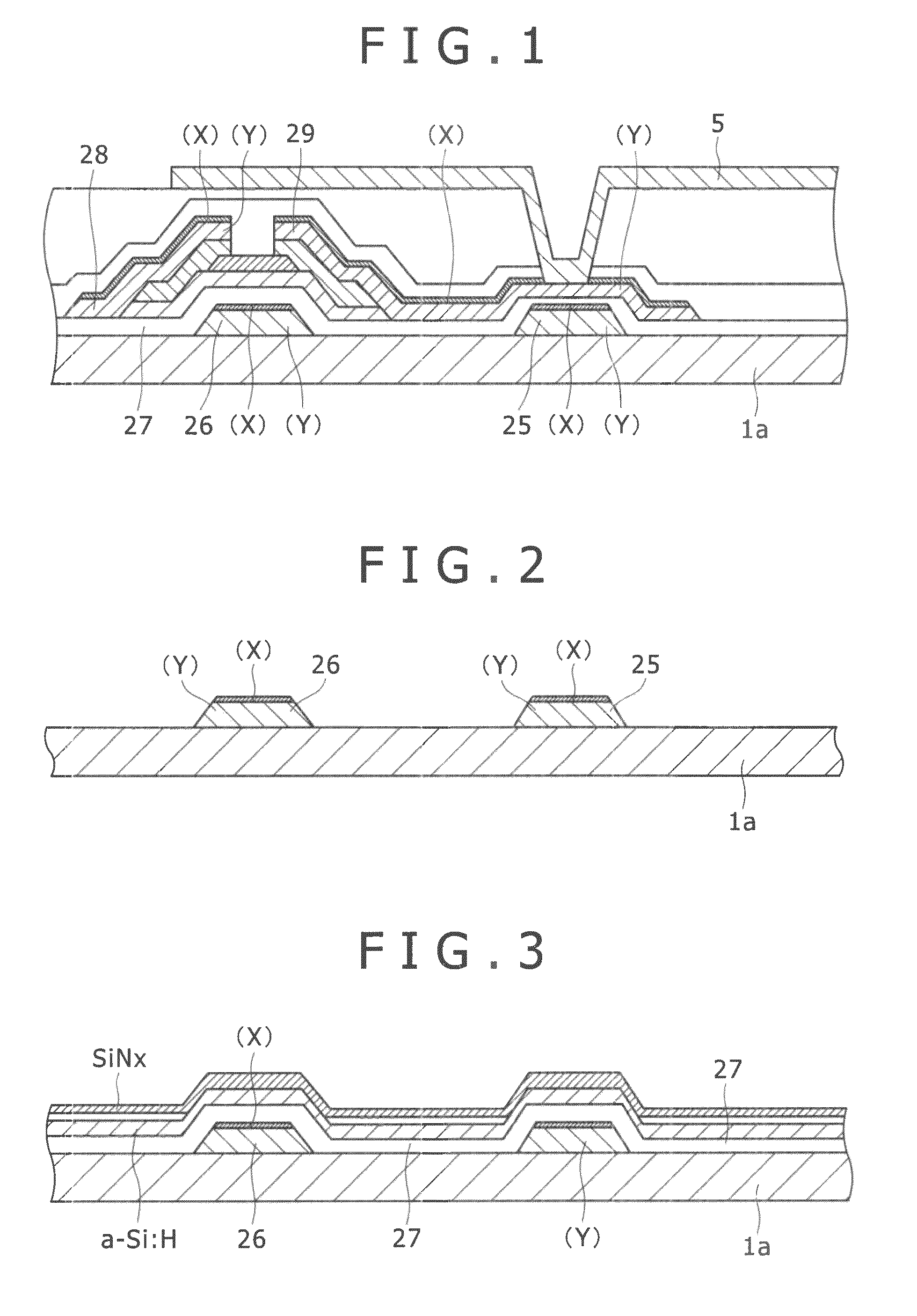
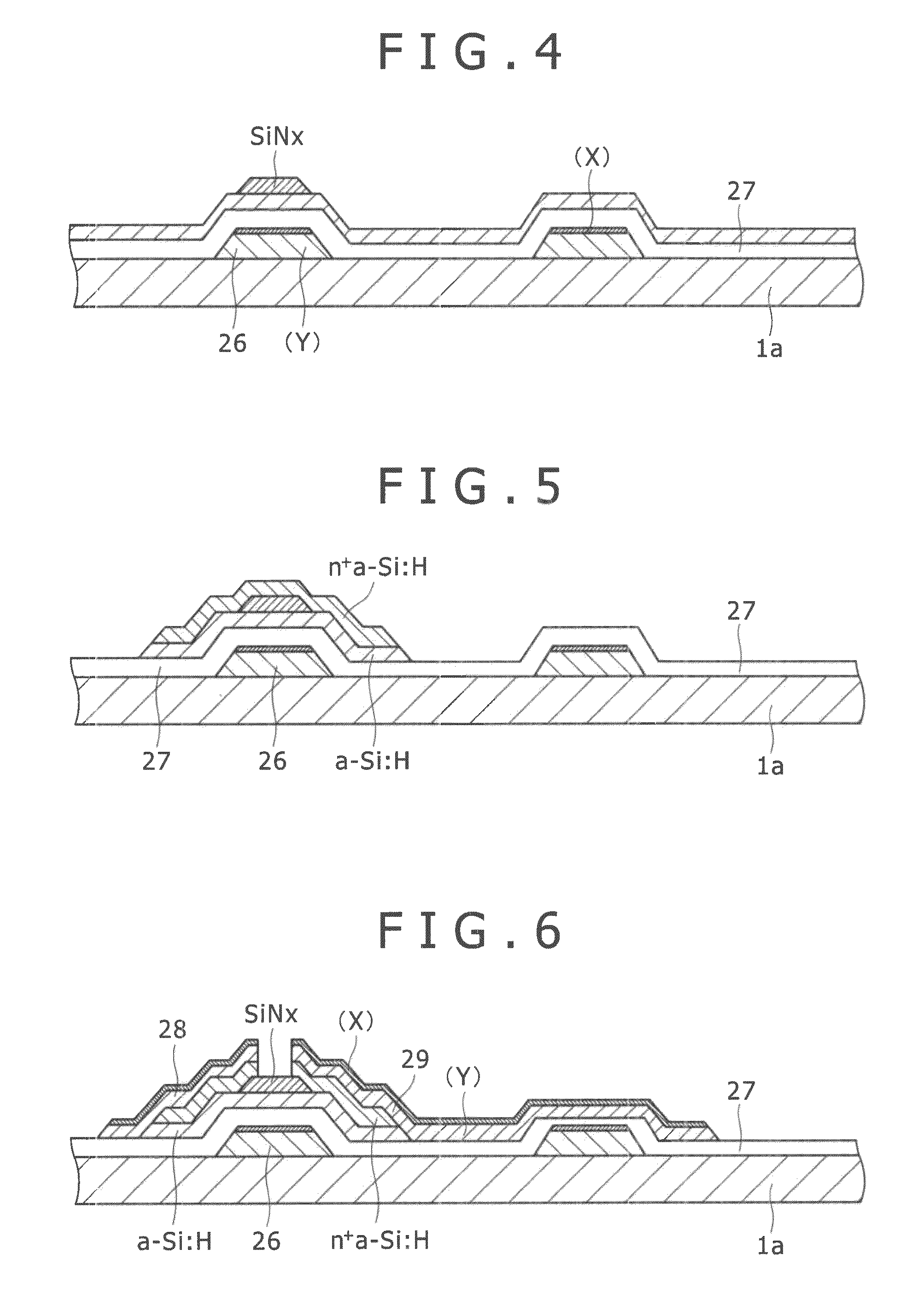
[0096]Cu alloy films each having the multilayer structure, which includes the first layer (Y) composed of a Cu alloy containing various elements shown in Table 1 and the second layer (X) composed of pure Cu, were produced as described below by a sputtering method. In Table 1, each of Nos. 3 to 16 represents an example in which Mn was added as the element of which the first layer (Y) was composed, No. 17 represents an example in which Bi was added, each of Nos. 18 to 21 represents an example in which Ni was added, each of Nos. 21 to 23 represents an example in which Zn was added, each of Nos. 24 and 25 represents an exa...

example 2

[0125]In the present example, the adhesiveness of each of the samples (present invention examples and comparative examples), which had used soda-lime glass and been produced in the following way, was investigated after the DC stress test and the peeling test. The DC stress test is a test method for checking a change in the leak current between electrodes and a change in the appearance, such as occurrence of peel off and formation of a foreign substance, while patterns electrically spaced apart from each other with a constant distance between them, are being maintained in a state of constant electric field strength being held between the patterns when a stress, which is a constant drive voltage (direct current), is applied between them. The DC stress test is useful as a test method in which an abnormality in the wiring, occurring due to the transfer of an electrical charge by a normal panel operation, can be checked in a short period of time by applying, in constant temperature and h...

example 3

[0135]In the present example, Mn was used as the element of which the first layer (Y) was composed, and influences on the adhesiveness to the glass substrate and the electrical resistivity by the content of Mn and the thickness of the first layer (Y) were investigated further in detail.

(1) Evaluation of Adhesiveness to Glass Substrate

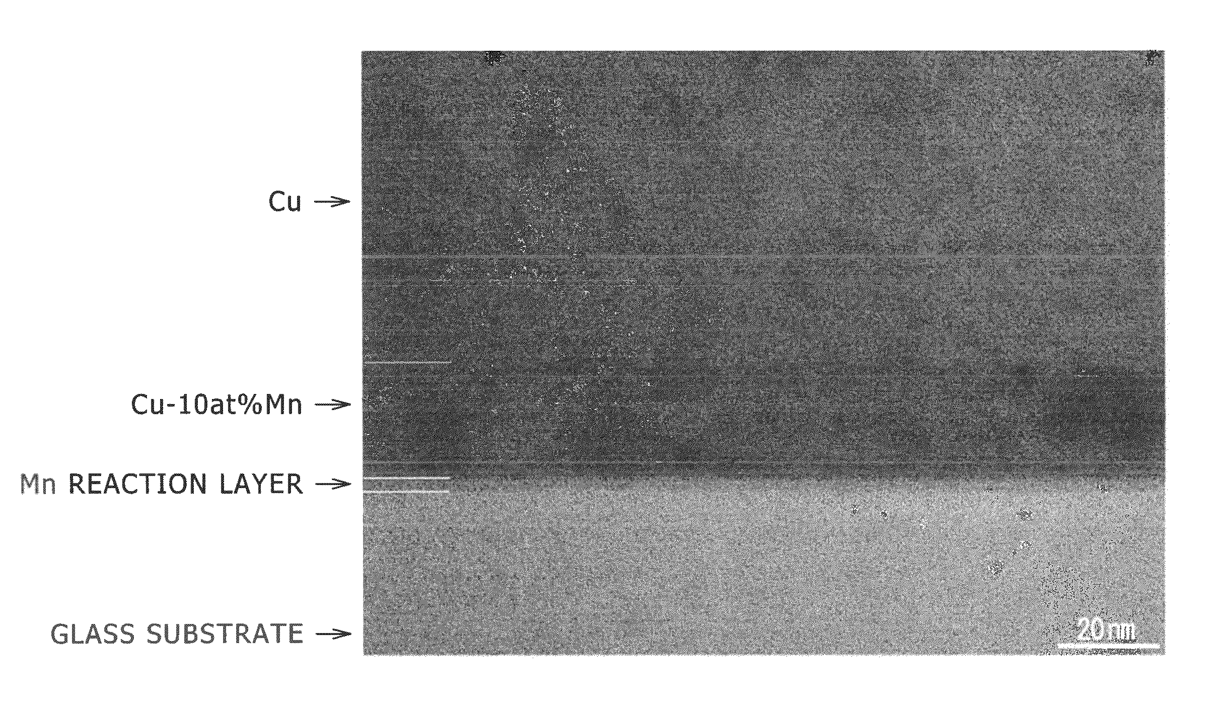
[0136]The multilayer film including the first layer (Y) and the second layer (X) was formed on a glass substrate in the same way as Example 1, except that EAGLE 2000 (size: 4 inches in diameter×0.7 mm in thickness) made by Corning Incorporated was used as the glass substrate, the thickness of the first layer (Y) was changed between 5 and 100 nm, and that of the second layer (X) was made constant at 500 nm. After the multilayer film was formed, a heat treatment was further performed at 320° C. for 5 minutes under 1 Pa of nitrogen atmosphere by using a CVD apparatus. Subsequently, cuts were made in a grid pattern of 5×5 cells at intervals of 1 mm on the s...


PUM

PropertyMeasurementUnit
thicknessaaaaaaaaaa
thicknessaaaaaaaaaa
taper angleaaaaaaaaaa

Abstract

A display device is provided with a Cu alloy film having high adhesiveness to a transparent substrate and a low electrical resistivity. The Cu alloy film for the display device is directly brought into contact with the transparent substrate, and the Cu alloy film has the multilayer structure, which includes a first layer (Y) composed of a Cu alloy containing, in total, 2-20 atm % of at least one element selected from among a group composed of Zn, Ni, Ti, Al, Mg, Ca, W, Nb, and Mn, and a second layer (X) which is composed of pure Cu or substantially a Cu alloy having Cu as the main component and has an electrical resistivity lower than that of the first layer (Y). The first layer (Y) is brought into contact with the transparent substrate.

Description

TECHNICAL FIELD[0001]The present invention relates to a display device with a Cu alloy film that is used in a display device, such as a liquid crystal display or organic electroluminescence display, and in particular, to a display device with a Cu alloy film excellent in the adhesiveness to a transparent substrate, such as a glass substrate.BACKGROUND ART[0002]Conventionally, aluminum (Al) alloy films have been used in the wiring of the display devices represented by liquid crystal displays. However, with the growth in size and the high definition of the display devices, problems resulting from a fact that a wiring resistance is large, such as signal delay and electrical power loss, are coming to the surface. Accordingly, copper (Cu) having a resistance lower than that of Al attracts attention as a wiring material. The electrical resistivity of Cu is as low as 1.6×10⁻⁶ Ω*cm, whereas that of Al is 2.5×10⁻⁶ Ω*cm.[0003]However, Cu has the problem that the adhesiveness thereof to a glas...

Claims


Application Information

Patent Timeline
Patent Type & Authority Patents(United States)
IPC IPC(8): H01L51/00
CPCB32B15/01C22C9/00C23C14/025C23C14/14G02F1/136286H01L23/53233H01L23/53238H01L29/458H01L29/4908H01L27/124H01L2924/0002G02F1/1368G02F2001/13629G02F2001/136295H01L2924/00G02F1/13629G02F1/136295H01L27/1214
Inventor GOTO, HIROSHIMIKI, AYATOMIHISA, KATSUFUMIOCHI, MOTOTAKAONISHI, TAKASHIKUGIMIYA, TOSHIHIRO
Owner KOBE STEEL LTD
Why Eureka
Try Eureka