Photo induced enhanced field electron emission collector

a photo-induced enhanced field and electron emission collector technology, applied in the field of light energy collection, can solve the problems of limited physical energy collection efficiency of pv technology, high cost of materials and manufacturing process, high cost of pure wafer production, etc., and achieve the effect of removing quantum bandgap restrictions, and improving the collection efficiency of electromagnetic radiation

Inactive Publication Date: 2013-08-13
PACIFIC INTEGRATED ENERGY
View PDF105 Cites 8 Cited by
  • Summary
  • Abstract
  • Description
  • Claims
  • Application Information

AI Technical Summary

Benefits of technology

[0019]The system and method disclosed herein improve the collection efficiency of electromagnetic radiation in general and more specifically the collection efficiency of visible light by 1) removing the quantum bandgap restrictions and utilizing a spectrum of electromagnetic radiation (e.g., for visible wavelengths, utilizing the entire visible and near visible spectrum, and 2) lowering the resistance of the free electrons. Additionally, the disclosed system and method do not require semiconductor materials, which results in devices that can be significantly less expensive than traditional semiconductor based photovoltaics.
[0023]The conical structures are inverted such that the base of the structure is at the top and the structure tapers downwardly. The base at the top faces the source of solar or other light energy. Preferably, the top base diameter (or other cross-sectional dimension) is on the order of the longest wavelength of collected light, which may comprise the infrared (IR) portion of the electromagnetic spectrum or the visible through ultraviolet (UV) portion of the spectrum. For visible and infrared light, the waveguide base, the wavelength is in a range of approximately 900 nanometers to 750 nanometers. The wavelengths are shorter for ultraviolet light. The sloping conical geometry creates an environment where each wavelength of the incident spectrum has a trap region with a respective diameter in the cone corresponding to each wavelength of light.

Problems solved by technology

PV technology is limited physically to less than 33% energy collection efficiency by bandgap energy collection limitations and by semiconductor electrical resistance.
The biggest cost issues associated with semiconductor-based PV are the cost of materials and the cost of the manufacturing process.
The material costs include the high cost to produce pure wafers and the use of rare and expensive materials.
The manufacturing costs include the huge capital cost to build a semiconductor facility, the control of toxic materials used and the cleanliness requirement to prevent any impurities from doping the product while under manufacture.
The large area requirement provides an inherent limitation to devices that use expensive processes because of the surface area cost to generate PV-based solar energy.
Therefore, the cost restrictions of inorganic-based PVs limit the ability to provide a significant portion of the US and world demands for electricity without a major paradigm shift in the way the PV devices are produced.
Another major downside for current PV technology is the use of toxic materials during the processing steps and in the end materials produced, particularly with respect to the newer triple-junction cells.
After the end of life of prior art PV devices, the toxic materials create an environmental disposal problem.
Such solar thermal methods have thermal loses.
Typically, solar thermal energy requires large operations to reach economic viability, which requires the system deployment to be located far from the source of demand.
This requires long-distance transmission lines that can have transmission losses as great as 30%.
Furthermore, the transmission lines and the supporting towers add cost in land and materials, and may have a negative environmental impact on the surfaces underlying the transmission lines.
Such devices have a net energy loss and amplify a signal using an external power source.
These devices consume more energy then they produce and are not useful as energy collectors.
As promising as these new technologies are, most are restricted to collecting light using discrete quantum energy bands, which imposes the same inherent efficiency limitations as semiconductor PV technologies.
As with inorganic semiconductors, this approach has a downside because each new well or junction creates a layer that can interfere with (mask) the well or junction below it and increase the path length of both the light and the free charge, which increases the losses from absorption and electrical resistance.
Furthermore, nanotechnology and quantum dots still have issues with toxicity, with the ability to manufacture and with efficiency.

Method used


Image

  • Photo induced enhanced field electron emission collector
  • Photo induced enhanced field electron emission collector
  • Photo induced enhanced field electron emission collector

Examples


Embodiment Construction

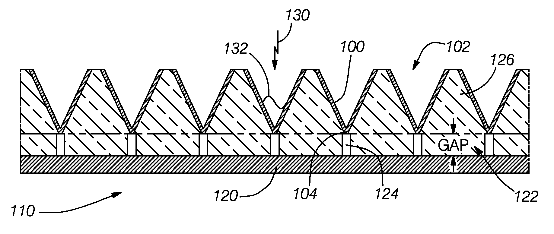
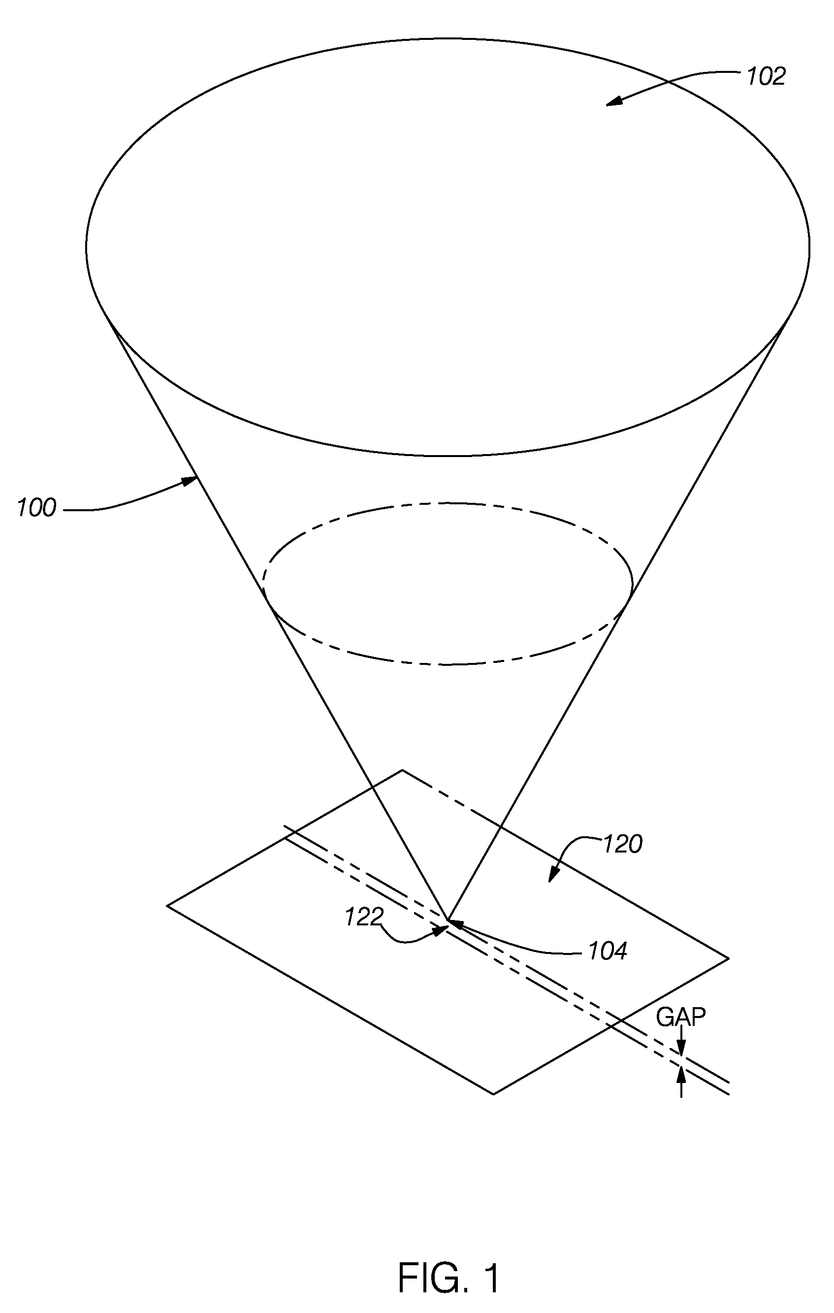
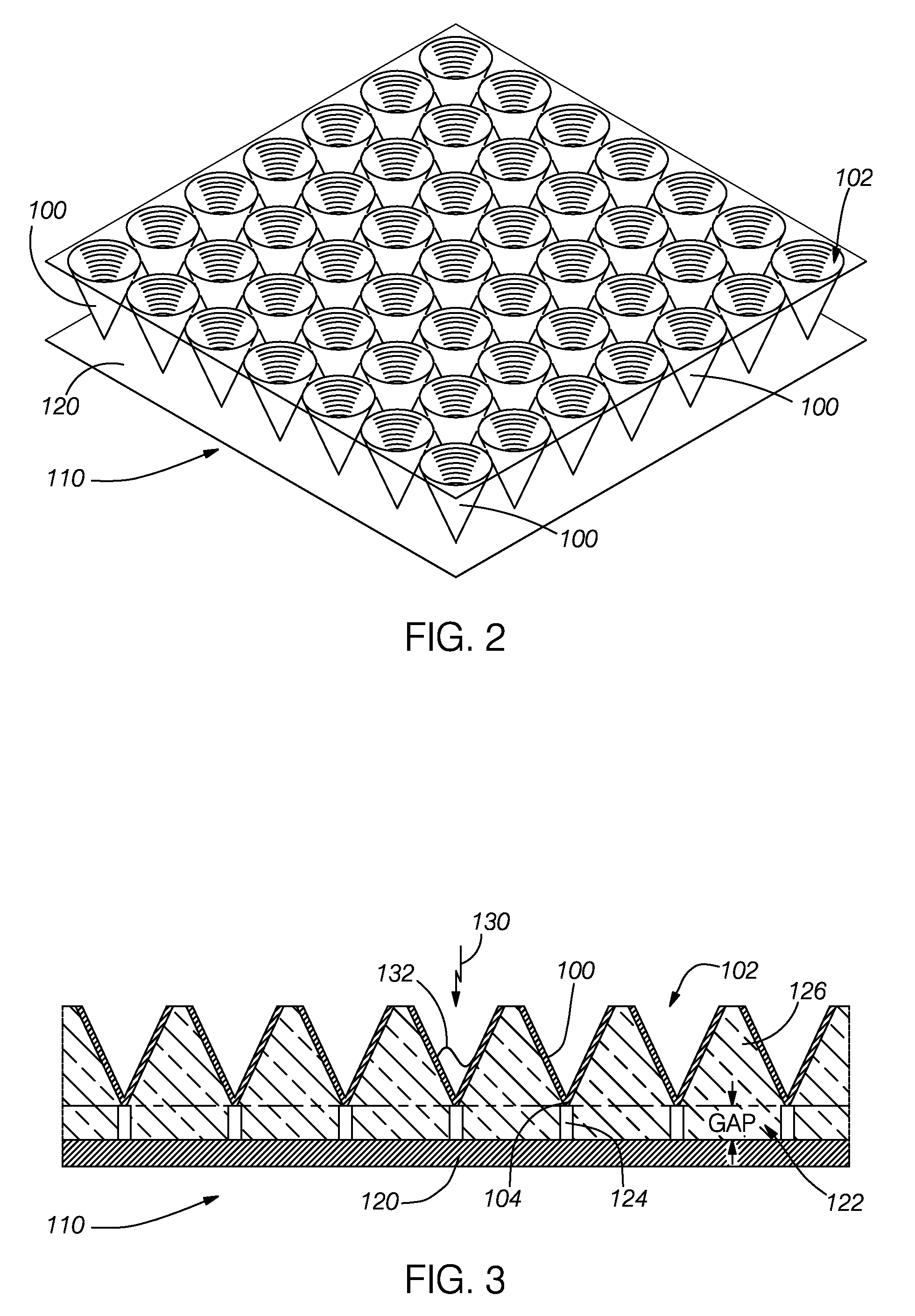
[0036]The drawings and the following description illustrate preferred embodiments of a system and method for implementing the present invention. Other shapes and configurations may also be used to create the disclosed effect of collecting the electric field from the electromagnetic wave and funneling the electric field to a localized field region above a conducting plane were electrons are emitted from the distress field point or line.

[0037]FIG. 1 illustrates a perspective view of a conical waveguide collecting structure 100 of a preferred embodiment of the system and method disclosed herein. The collecting structure comprises a conducting material that tapers from a base 102 to a point 104. Preferably, the conducting material is a thin conducting film. For example, the conducting material advantageously comprises graphene (a honeycomb crystal lattice of densely packed carbon atoms in a one-atom-thick planar sheet) or other carbon materials that are electrical conducting. The conduc...


PUM


Abstract

An electromagnetic energy collector and sensor use enhanced fields to emit electrons for energy collection. The collector and sensor collect energy from visible light, infrared radiation and ultraviolet electromagnetic radiation. The collector and sensor include a waveguide with a geometry selected to enhance the electric field along a conductor to create a high, localized electric field, which causes electron emission across a gap to a return plane.

Description

RELATED APPLICATIONS[0001]This application claims the benefit of priority under 35 USC 119(e) to U.S. Provisional Patent Application No. 60 / 985,841, filed on Nov. 6, 2007, which is incorporated in its entirety by reference herein.BACKGROUND OF THE INVENTION[0002]1. Field of the Invention[0003]The invention disclosed herein relates generally to the field of electromagnetic energy collection, and, more specifically, relates to light energy collection.[0004]2. Description of the Related Art[0005]The system and method disclosed herein produce energy from sunlight by harvesting electromagnetic waves using a field concentrating method to create an electron emission from a distressed field source.[0006]A combination of increasing worldwide energy demand, limited energy resources that are unable to keep up with the demand and the environmental impact of harvesting nonrenewable energy fossil fuels has created an increasing demand for clean affordable renewable energy.[0007]One source of rene...

Claims


Application Information

Patent Timeline
Patent Type & Authority Patents(United States)
IPC IPC(8): H01L31/00
CPCG02B5/008H01Q15/02H01Q15/0073H01J29/04H01L31/0522F24J2/00
Inventor LAYTON, PHILLIP J.
Owner PACIFIC INTEGRATED ENERGY
Why Eureka
Try Eureka