
Mask, manufacturing method thereof and mask haze monitoring method

a mask and manufacturing method technology, applied in the field of masks, can solve the problems of difficult to avoid, severely affect process yield, and always concern about mask contamination, and achieve the effects of effective detection of mask haze, removal of haze, and improved product yield

Active Publication Date: 2013-10-22
SEMICONDUCTOR MANUFACTURING INTERNATIONAL (BEIJING) CORP
View PDF2 Cites 2 Cited by
  • Summary
  • Abstract
  • Description
  • Claims
  • Application Information

AI Technical Summary

Benefits of technology

[0010]In view of the above, it is needed to provide an improved solution for detecting mask haze, which can effectively detect mask haze in time, so as to remove the haze as early as possible and improve product yield.
[0035]Many benefits are achieved by way of the present invention over the conventional techniques. For example, the mask according to the present invention provides the ability to monitor mask haze online, thereby effectively detecting mask haze in time.

Problems solved by technology

During manufacturing processes, mask contamination has always been a concern.
Since the pattern in a mask is repeatedly transferred onto a wafer, mask contamination will cause defects in a large number of semiconductor chips, and severely affects process yield.
Among different types of mask contamination, haze is the most common contamination which has the severest effect and is difficult to be avoided.
Generally, sulphuric acid is used in mask cleaning, which may cause sulphate ions to be left on the mask.
As the crystal grows to a certain size (for example, when its size is equivalent to the pattern size on the mask), the precision of pattern transfer will be affected, which consequently lowers the yield of integrated chips.
With the continuous shrinking of the size of semiconductor devices, exposure wavelength in photolithography decreases continuously, and thus the effect by haze becomes increasingly severer.
For advanced integrated circuit (IC) processes, since more and more semiconductor layers require the use of a 193 nm exposure wavelength, the probability of occurrences of chip defects caused by mask haze will significantly increase.
However, this inspection method is very expensive and time consuming.
The inspection of one piece of mask usually takes 2 to 4 hours, which not only decreases the production efficiency of semiconductor devices, but also increases the cost.
Moreover, since inspection of the mask is regularly carried out offline, it is hard to find mask haze in time.
However, this method is time consuming, requires additional manpower, and does not provide sufficient accuracy.
In addition, this method is only capable of detecting mask haze of large size which has already resulted in chip defects, but fails to detect the mask haze before the mask haze causes chip defects.
In practice, when mask haze is detected by means of this method, a large number of defect chips have already been produced, which leads to yield loss.

Method used


Image

  • Mask, manufacturing method thereof and mask haze monitoring method
  • Mask, manufacturing method thereof and mask haze monitoring method
  • Mask, manufacturing method thereof and mask haze monitoring method

Examples


Embodiment Construction

[0045]Various exemplary embodiments of the present invention will now be described in detail with reference to the drawings. It should be noted that the relative arrangement of the components and steps, the numerical expressions, and numerical values set forth in these embodiments do not limit the scope of the present invention unless it is specifically stated otherwise.

[0046]Meanwhile, it should be understood that, for the convenience of description, each component in the figures has not been necessarily drawn to scale.

[0047]The following description of at least one exemplary embodiment is merely illustrative in nature and is in no way intended to limit the invention, its application, or uses.

[0048]Techniques, methods and apparatus as known by one of ordinary skill in the relevant art may not be discussed in detail but are intended to be part of the specification where appropriate.

[0049]In all of the examples illustrated and discussed herein, any specific values should be interpret...


PUM

PropertyMeasurementUnit
distanceaaaaaaaaaa
wavelengthaaaaaaaaaa
transmittanceaaaaaaaaaa

Abstract

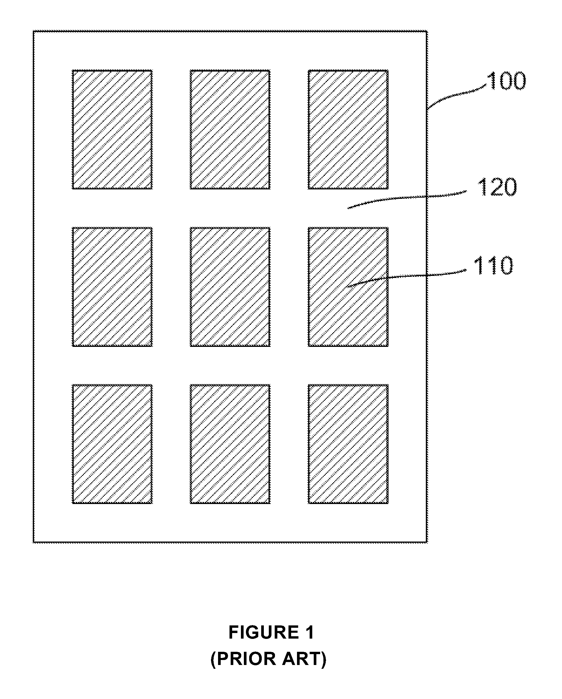
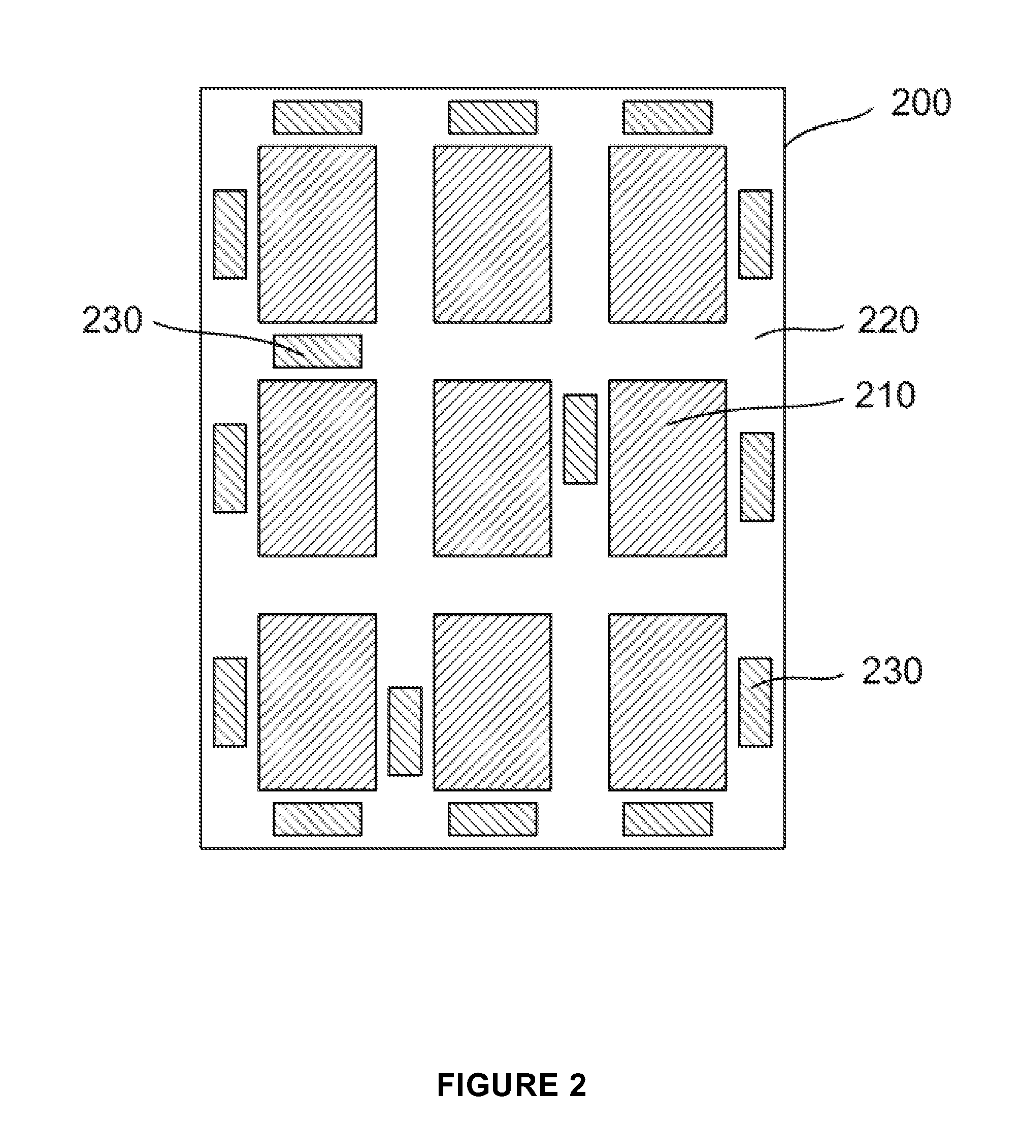
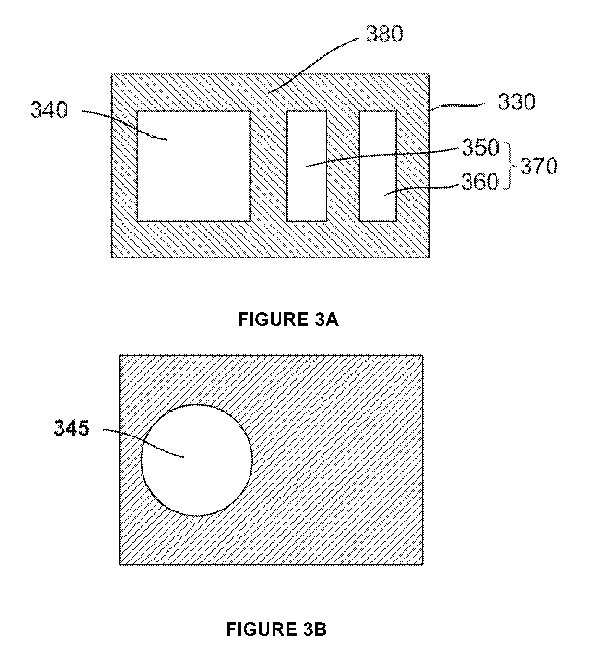
A mask and methods for making the mask and monitoring mask haze using the mask are provided. The mask includes chip areas that are separated by scribe lanes. A scribe lane includes a monitoring area that contains a primary pattern and an associated assist feature. The assist feature includes two parallel scattering bars. Regions in the monitoring area other than the primary pattern and the associated assist feature are covered with a phase shift layer having a transmittance smaller than that of the primary pattern and the assist feature. When the mask is exposed to a light source, the assist feature is not transferred onto a wafer but cooperates with the primary pattern to generate a primary transferred pattern on the wafer. When a region between the two scattering bars has mask haze thereon, a defect identification pattern is generated on the wafer near the primary transferred pattern following exposure.

Description

CROSS-REFERENCES TO RELATED APPLICATIONS[0001]This application claims priority to Chinese Patent Application No. 201110330676.3, filed on Oct. 27, 2011 and entitled “Mask, Manufacturing Method thereof and Mask Haze Monitoring Method”, which is incorporated herein by reference in its entirety.BACKGROUND OF THE INVENTION[0002]1. Field of the Invention[0003]The present invention generally relates to the field of semiconductor manufacturing, and more specifically, to a mask used in a semiconductor manufacturing process and methods for making the mask and for the haze monitoring using the mask.[0004]2. Description of the Related Art[0005]During the manufacture of semiconductor integrated circuits, photolithography is a very important process. In the photolithography, a pattern (such as a pattern of metal wires or contact holes) with a predefined design is firstly formed on one or more masks, and the pattern on the mask is then transferred onto a photoresist layer on a wafer using a photo...

Claims


Application Information

Patent Timeline
Patent Type & Authority Patents(United States)
IPC IPC(8): G03F1/26G03F1/36
CPCG03F1/38G03F1/44G03F1/84H01L2924/0002H01L2924/00H01L22/30H01L23/544H01L2223/54426H01L2223/5446G03F1/50
Inventor HU, HUAYONGZHANG, SHIJIAN
Owner SEMICONDUCTOR MANUFACTURING INTERNATIONAL (BEIJING) CORP
Learn More