Method for correcting amplitude and phase offsets in a sigma-delta modulator and sigma-delta modulator implementing said method

a sigma-delta modulator and amplitude offset technology, applied in the field of sigma-delta modulators and modulators implementing methods, can solve the problems of insufficient capacity of conventional adcs to sample/quantify input signals both rapidly and accurately, and the duration required for stabilization thus being too long with respect to the sampling period, so as to improve the accuracy of an adc, minimize errors, and improve time-domain precision

Inactive Publication Date: 2013-12-24
THALES SA
View PDF9 Cites 6 Cited by
  • Summary
  • Abstract
  • Description
  • Claims
  • Application Information

AI Technical Summary

Benefits of technology

[0005]A method called sigma-delta modulation provides for improving the precision of an ADC locally around a frequency, if necessary around a high frequency. The basic principle is to make the digital output signal vary arbitrarily, or to “modulate” it, so as to minimize the error for any spectral component contained in the relevant band (which depends on the use), even if it means that samples of the digital output signal can appear unrepresentative of the analog input signal. To this end, sigma-delta modulation requires by principle that the signal be strongly oversampled, which can be done only on a small number of bits. This amounts to improving the time-domain precision by cutting the signal into a large number of samples but, as explained earlier, at the cost of a reduction in amplitude precision due to the increase in sampling frequency. However, by relying on oversampling, the digital output signal can be modulated in order to minimize the power of this quantization noise in a defined frequency band.

Problems solved by technology

But in the field of microwave frequencies, when the frequency of the input signal is of the order of a few gigahertz, the dynamics of conventional ADCs, i.e. their capability to sample / quantize the input signal both rapidly and accurately turns out to be markedly inadequate.
First of all, this is due to the inadequate rise time of an internal component of ADCs called the sample / hold circuit.
It may be difficult for a sample / hold circuit to stabilize an input signal with a view to quantizing it if it is at too high a frequency, the duration required for this stabilization hence being too long with respect to the sampling period.
This introduces errors, i.e. digital samples can be unrepresentative of the analog signal.
This intrinsically generates an error due to the lack of precision before the quantization of the amplitude of each sample.
Consequently, the error inherent to the digitization method of a conventional ADC at high sampling frequency is the sum of the error described, related to the rapidity defect of the sample / hold circuit, and of the quantization rounding error which reflects the difference between the signal thus sampled / held and its quantized digital representation.
Thus, at high frequency, the difference between the signal represented digitally at the output and the analog signal at the input becomes non-negligible and the precision of the ADC is no longer satisfactory.
They are therefore not suitable for use in very high-frequency applications demanding good digital precision, such as radars for example.
This amounts to improving the time-domain precision by cutting the signal into a large number of samples but, as explained earlier, at the cost of a reduction in amplitude precision due to the increase in sampling frequency.
Thus, even if an overall significant quantization noise is intrinsically generated in sigma-delta modulation, and this regardless of the frequency of the signal at the input, at least this quantization noise is of low power close to the frequency of use.
For example, if a variation in the loop delay involves a phase offset between −π and π in the loop bandwidth, it is probable that the modulator has become unstable.

Method used


Image

  • Method for correcting amplitude and phase offsets in a sigma-delta modulator and sigma-delta modulator implementing said method
  • Method for correcting amplitude and phase offsets in a sigma-delta modulator and sigma-delta modulator implementing said method
  • Method for correcting amplitude and phase offsets in a sigma-delta modulator and sigma-delta modulator implementing said method

Examples


Embodiment Construction

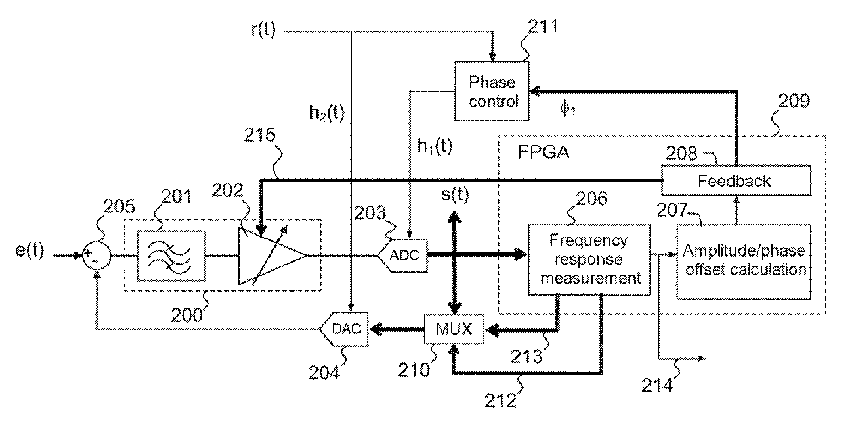
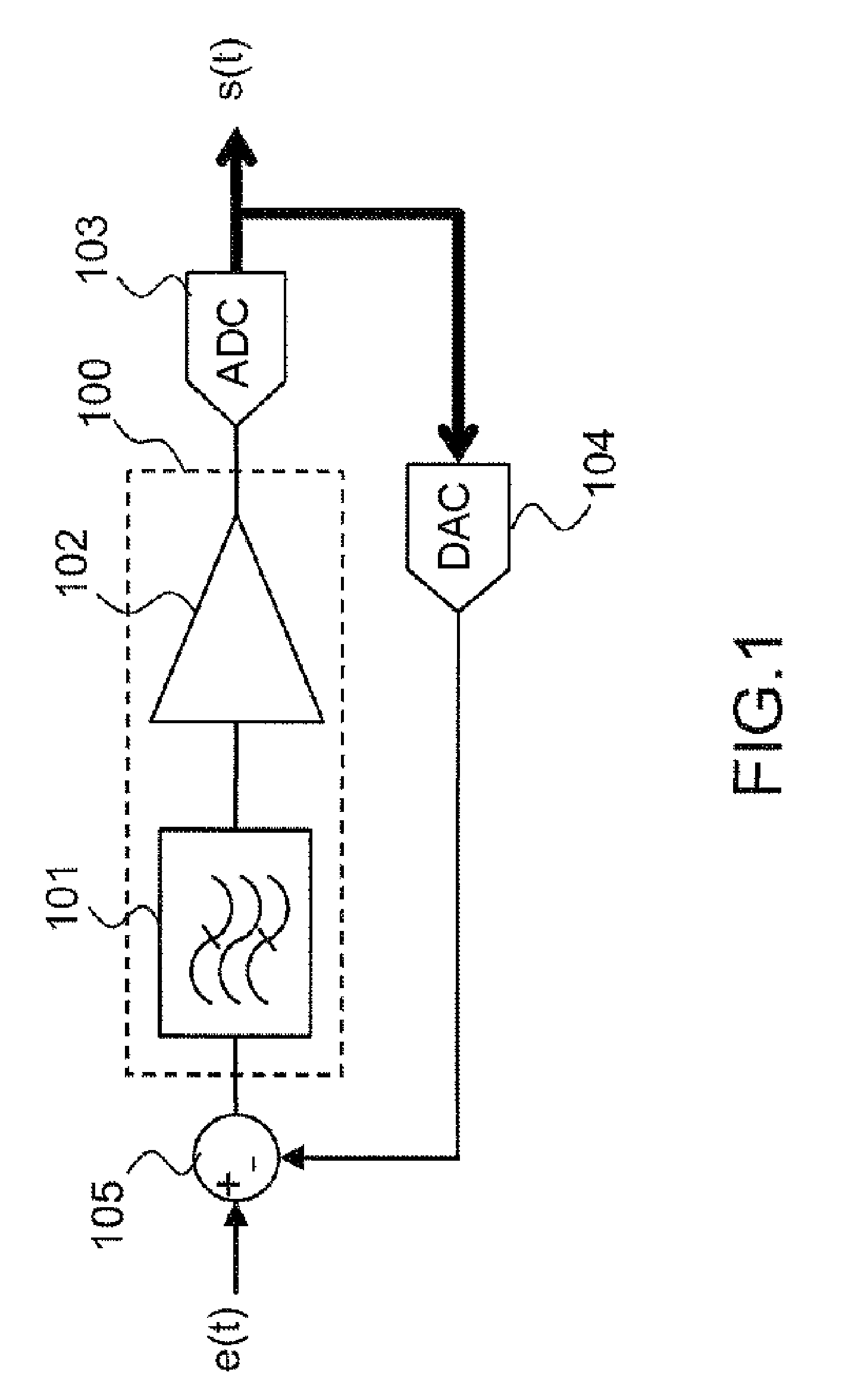
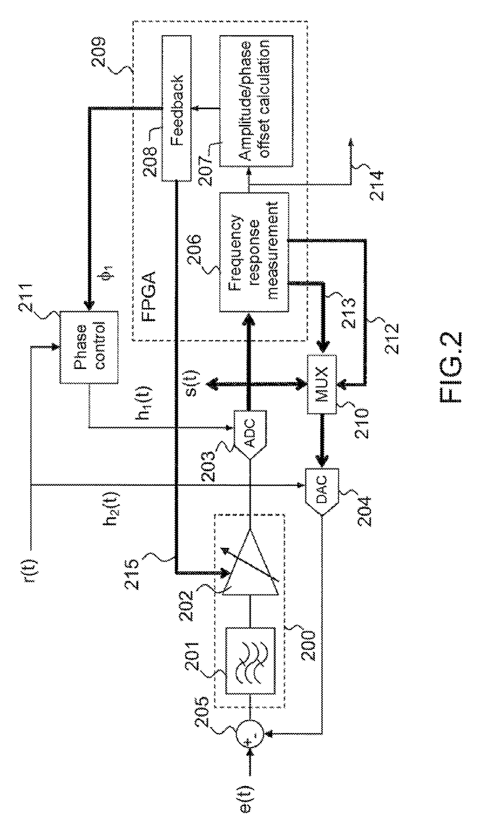
[0025]FIG. 1 presents an example sigma-delta modulator. As explained previously, the role of a continuous-time sigma-delta modulator is two-fold. A first role is to sample and digitize at high sampling frequency an analog signal e(t) with a small number of bits, i.e. less than the theoretical number required to reach a given signal-to-noise ratio. A second role is to shape the quantization noise so that the spectral density of this noise in the useful band of the signal to be converted is compatible with the signal-to-noise ratio aimed at after decimation. To this end, a continuous-time bandpass sigma-delta modulator is comparable to a feedback loop. An integrator 100 itself composed of a bandpass filter 101 and an amplifier 102 has the role of integrating and amplifying the error in the useful band of the signal. The loop comprises an ADC converter 103 producing the output s(t) of the modulator. The output s(t), i.e. the encoded signal, is then looped back to a DAC converter 104. A...


PUM


Abstract

In a method for correcting amplitude and phase offsets in a sigma-delta modulator having a loop including an integrator with a filter and an amplifier, an analog-to-digital converter, a digital-to-analog converter, and an adder-subtractor, an open-loop amplitude/phase frequency response of the modulator is estimated digitally. A phase offset value and an amplitude offset value are calculated by comparing the estimated open-loop amplitude/phase response with a reference amplitude/phase frequency response. The phase and gain offsets of the loop are then compensated for according to the estimated offset values. A sigma-delta modulator implements the method.

Description

CROSS-REFERENCE TO RELATED APPLICATIONS[0001]This application is a National Stage of International patent application PCT / EP2009 / 064322, filed on Oct. 29, 2009, which claims priority to foreign French patent application No. FR 08 06077, filed on Oct. 31, 2008, the disclosures of which are incorporated by reference in their entirety.FIELD OF THE INVENTION[0002]The present invention relates to a method for correcting amplitude and phase offsets in a sigma-delta modulator and a modulator implementing the method. It applies notably to the field of signal processing and electronics.BACKGROUND OF THE INVENTION[0003]The conversion of an analog signal into a digital signal has become a conventional operation in present-day electronic circuits, by virtue of standard commercially available components generally grouped together under the acronym ADC, for “Analog-to-Digital Converter”. A signal e(t) is represented, varying continuously in time and able to take any value in a form s(t) sampled i...

Claims


Application Information

Patent Timeline
Patent Type & Authority Patents(United States)
IPC IPC(8): H03M1/06
CPCH03M3/354H03M3/37H03M3/402H03M3/424H03M3/456
Inventor HODE, JEAN-MICHEL
Owner THALES SA
Why Eureka
Try Eureka