Semiconductor device and method of manufacturing same

a semiconductor device and semiconductor technology, applied in the field of semiconductor devices, can solve the problems of difficult to achieve crystallinity or impurity concentration, difficult operation of the semiconductor device, and long time-consuming device manufacturing, so as to reduce the on resistance of the semiconductor device and maintain normal-off characteristics. , the effect of simple step

Active Publication Date: 2014-02-04
RENESAS ELECTRONICS CORP
View PDF12 Cites 5 Cited by
  • Summary
  • Abstract
  • Description
  • Claims
  • Application Information

AI Technical Summary

Benefits of technology

[0008]One of them is to form the electron supply layer 403 selectively, that is, only in a region other than the gate region. This method enables formation of the structure of the MIS field effect transistor 440 precisely, but requires twice epitaxial growth until the formation of the electron transit layer 402 and one and after the formation of the electron supply layer 403. As a result, it takes much time for manufacturing the device compared with a related-art MIS field effect transistor. As the step premised on mass production, twice growth is not desired from the standpoint of production efficiency. In addition, in the second growth step, a portion of the gate region not subjected to epitaxial growth must be protected with a mask material such as silicon oxide film. It is therefore difficult to achieve desired crystallinity or impurity concentration. Moreover, formation of defects or incorporation of impurities occurs at the re-growth interface and it deteriorates the mobility of a two dimensional electron gas at a hetero interface between the electron supply layer 403 and the electron transit layer 402, which may be a cause for increasing the on resistance. Further, this formation method causes problems, which may be a factor for making the operation of the semiconductor device unstable, typified by current collapse due to response of defect states or impurity states. As a result, they may deteriorate the yield of the products.
[0015]The present invention makes it possible to achieve crystallinity of a semiconductor film desired for the electrical properties of a field effect transistor which is a nitride semiconductor device, a simple step enabling mass production, and a reduction in the on resistance of the semiconductor device while maintaining normally-off characteristics.

Problems solved by technology

As a result, it takes much time for manufacturing the device compared with a related-art MIS field effect transistor.
It is therefore difficult to achieve desired crystallinity or impurity concentration.
Moreover, formation of defects or incorporation of impurities occurs at the re-growth interface and it deteriorates the mobility of a two dimensional electron gas at a hetero interface between the electron supply layer 403 and the electron transit layer 402, which may be a cause for increasing the on resistance.
Further, this formation method causes problems, which may be a factor for making the operation of the semiconductor device unstable, typified by current collapse due to response of defect states or impurity states.
As a result, they may deteriorate the yield of the products.
In this method, however, the depth direction of recess etching cannot be controlled well because of the lack of an effective recess stopper.

Method used


Image

  • Semiconductor device and method of manufacturing same
  • Semiconductor device and method of manufacturing same
  • Semiconductor device and method of manufacturing same

Examples


first embodiment

[0025][First Embodiment]

[0026]The constitution of the semiconductor device 100 using a nitride semiconductor according to the present embodiment will next be described referring to drawings.

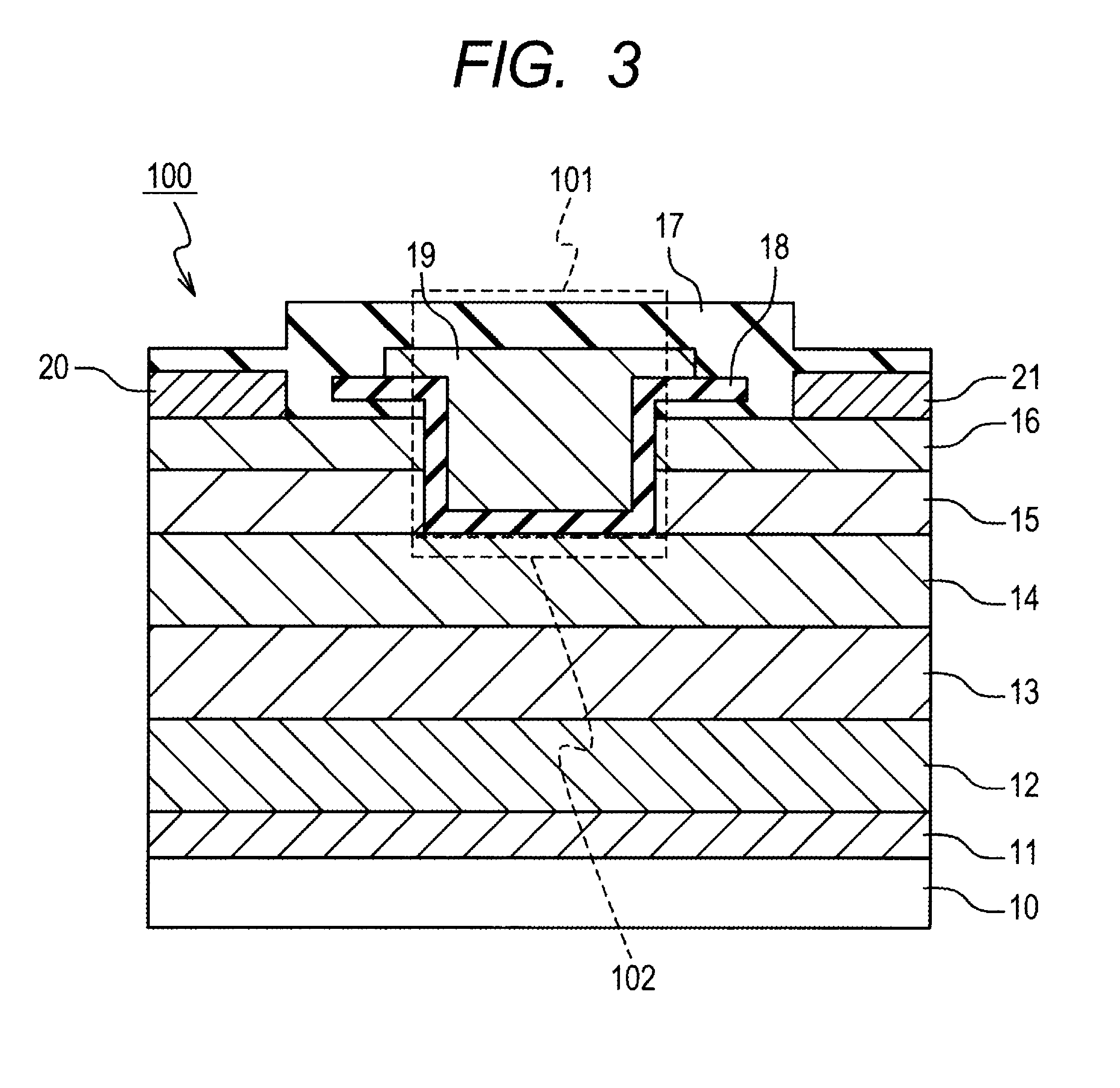
[0027]FIG. 3 is a cross-sectional view showing the structure of the semiconductor device 100 using a nitride semiconductor according to the present embodiment. The semiconductor device 100 in FIG. 3 is an MIS field effect transistor. As shown in FIG. 3, the semiconductor device 100 is equipped with a substrate 10, a nucleation layer 11, a buffer layer 12, an underlying layer 13, a second electron transit layer 14, a first electron transit layer 15, an electron supply layer 16, a semiconductor surface protecting film 17, a gate insulating film 18, a gate electrode 19, a source electrode 20, and a drain electrode 21.

[0028]In the present embodiment, silicon is used as the substrate 10. However, a substrate of another material such as GaN substrate, AlN substrate, sapphire substrate, or SiC substrate...

second embodiment

[0067][Second Embodiment]

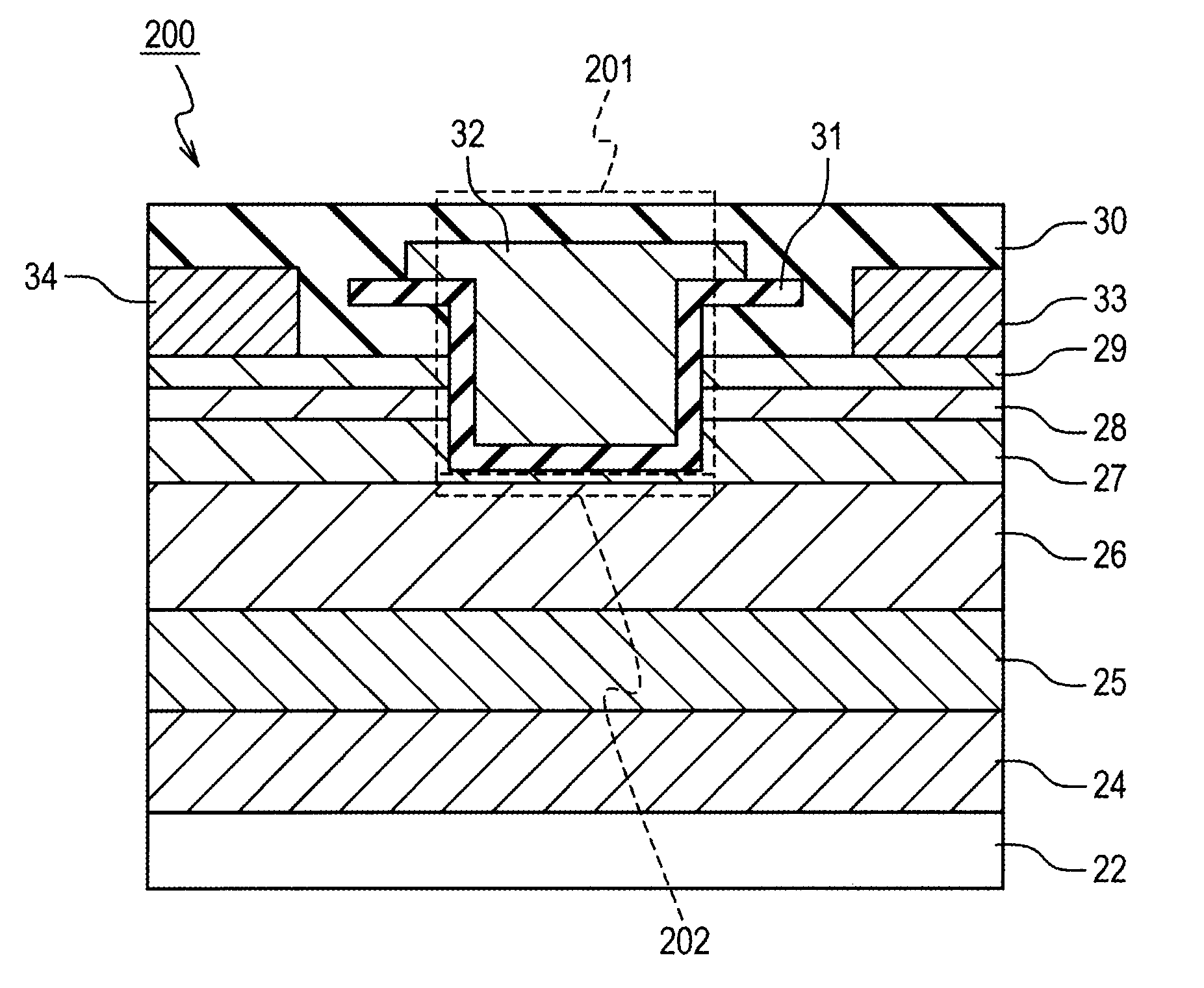
[0068]Referring to drawings, a description will next be made on the constitution of a semiconductor device 200 using a nitride semiconductor according to the present embodiment.

[0069]Referring to FIG. 4, the semiconductor device 200 is equipped with a substrate 22, a buffer layer 24, an underlying layer 25, a second electron transit layer 26, a first electron transit layer 27, a second electron supply layer 28, a first electron supply layer 29, a semiconductor surface protecting film 30, a gate insulating film 31, a gate electrode 32, a source electrode 33, and a drain electrode 34.

[0070]In the present embodiment, SiC is used as the substrate 22. However, another material may be used, depending on the intended use.

[0071]In the present embodiment, Al0.2Ga0.8N is used as the buffer layer 24. However, another material, another composition ratio, or a desired film thickness can be selected, depending on the intended use or a substrate used. It is also possible t...

third embodiment

[0109][Third Embodiment]

[0110]The constitution of a semiconductor device 300 using a nitride semiconductor according to the present embodiment will next be described referring to drawings.

[0111]FIG. 6 is a cross-sectional view illustrating the structure of the semiconductor device 300 using a nitride semiconductor according to the present embodiment. The semiconductor device 300 in FIG. 6 is an MIS field effect transistor. According to FIG. 6, the semiconductor device 300 is equipped with a substrate 10, a nucleation layer 11, a buffer layer 36, an underlying layer 37, a second electron transit layer 38, a first electron transit layer 39, an electron supply layer 40, a gate insulating film 18, a gate electrode 32, a source electrode 43, and a drain electrode 44.

[0112]In the present embodiment, Al0.3Ga0.7N is used as the buffer layer 36. However, depending on the intended use or a substrate used, another material, another composition ratio, or a desired film thickness may be selected...


PUM


Abstract

Object of the invention is to reduce the on resistance between source and drain of a nitride semiconductor device. Between a nitride semiconductor layer lying between source and drain regions and a nitride semiconductor layer serving as an underlying layer, formed is a material having an electron affinity greater than that of these nitride semiconductor layers and having a lattice constant greater than that of the nitride semiconductor layer serving as an underlying layer. As a result, an electron density distribution of a channel formed below a gate insulating film and that of a two-dimensional electron gas formed in a region other than the gate portion, when a gate voltage is applied, can be made closer in the depth direction, leading to reduction in on resistance.

Description

CROSS-REFERENCE TO RELATED APPLICATIONS[0001]The disclosure of Japanese Patent Application No. 2011-134270 filed on Jun. 16, 2011 including the specification, drawings and abstract is incorporated herein by reference in its entirety.BACKGROUND[0002]The present invention relates to a semiconductor device, in particular, to a normally-off type MIS field effect transistor using a nitride semiconductor and a method of manufacturing the device.[0003]Power semiconductor elements are used in power electronics semiconductor devices or high-frequency amplifiers. Power semiconductor elements are required to have low on resistance and high withstand voltage operation. To achieve such electrical properties, a nitride semiconductor having a greater band gap is used as an element material instead of conventionally used silicon. For example, Japanese Patent Laid-Open No. 2010-109086 discloses a nitride semiconductor element equipped with a first semiconductor layer of a p type nitride semiconducto...

Claims


Application Information

Patent Timeline
Patent Type & Authority Patents(United States)
IPC IPC(8): H01L29/78
CPCH01L29/518H01L29/66462H01L29/7787H01L29/2003H01L29/4236H01L21/28264
Inventor NAKAYAMA, TATSUO
Owner RENESAS ELECTRONICS CORP
Why Eureka
Try Eureka