Microcontroller controlled or direct mode controlled network-fabric on a structured ASIC

a microcontroller and network fabric technology, applied in the field of structured asics, can solve the problems of wasting time and effort, affecting the functionality of the system, and the components are no longer supported by modern eda (electronic design automation) software,

Active Publication Date: 2014-03-18
INTEL CORP
View PDF13 Cites 50 Cited by
  • Summary
  • Abstract
  • Description
  • Claims
  • Application Information

AI Technical Summary

Benefits of technology

[0049]A further aspect of the present invention is for an easy way of switching testing modes when testing a chip from an external device test mode to an internal processor test mode, both modes of testing using the same network-aware IO and connection fabric. Hence an aspect of the invention is to provide two ways of testing a Structured ASIC, a Direct Mode control under the control of an external testing apparatus control agent and an internal microprocessor-based Microcontroller Control under the control of an internal testing control agent such as a microprocessor; generically defining the control agent that directs the testing for both cases as a Tester.

Problems solved by technology

While the layout of each cell in a standard cell is predetermined, the circuit itself has to be uniquely constructed by connecting all layers to one another and the cells within each layer in a custom manner, which takes time and effort.
A simple PLD, historically called a programmable logic device, is much more limited in application, as they do not have a general interconnect structure.
These components are no longer supported by modern EDA (Electronic Design Automation) software and have very limited functionality.
However, optimizing multilevel synthesis logic is more difficult than optimizing two-level synthesis logic, and often employs heuristic techniques.
Design constraints in floorplanning include minimizing the silicon chip area and minimizing timing delay.
The determination of the MRST is in general an NP-complete problem—which is difficult to solve in a reasonable time.
For small numbers of terminals heuristic algorithms exist, but they are expensive in engineering cost to compute.
If a via is disabled, then it cannot practically conduct a signal, i.e., the via has very high resistance or does not physically exist.
If the clock signal arrives at different components at different times, there is clock skew.
Clock skew can be caused by many different things, such as wire-interconnect length, temperature variations and differences in input capacitance on the clock inputs of devices using the clock.
These are also the disadvantages of standard cell ASICs: they can be difficult to design, have longer development times, and higher NRE costs.
The disadvantages of FPGAs are that design size is limited to relatively small production designs, design complexity is limited, performance is limited, power consumption is high, and there is a high cost per unit.
These FPGA disadvantages are standard-cell advantages, as standard cells support large and complex designs, have high performance, low power consumption and low per-unit cost at a high volume.
The disadvantage of structured ASICs compared to FPGAs is that FPGAs do not require any user design information during manufacturing.
Fewer metal layers are needed for fabrication of a Structured ASIC, which dramatically reduces the turnaround time.
The unit cost of a Structured ASIC may be somewhat higher than a full custom ASIC, primarily due to the imperfect fit between design requirements and a standardized base layer, with certain I / O, memory and logic capacities.

Method used


Image

  • Microcontroller controlled or direct mode controlled network-fabric on a structured ASIC
  • Microcontroller controlled or direct mode controlled network-fabric on a structured ASIC
  • Microcontroller controlled or direct mode controlled network-fabric on a structured ASIC

Examples


Embodiment Construction

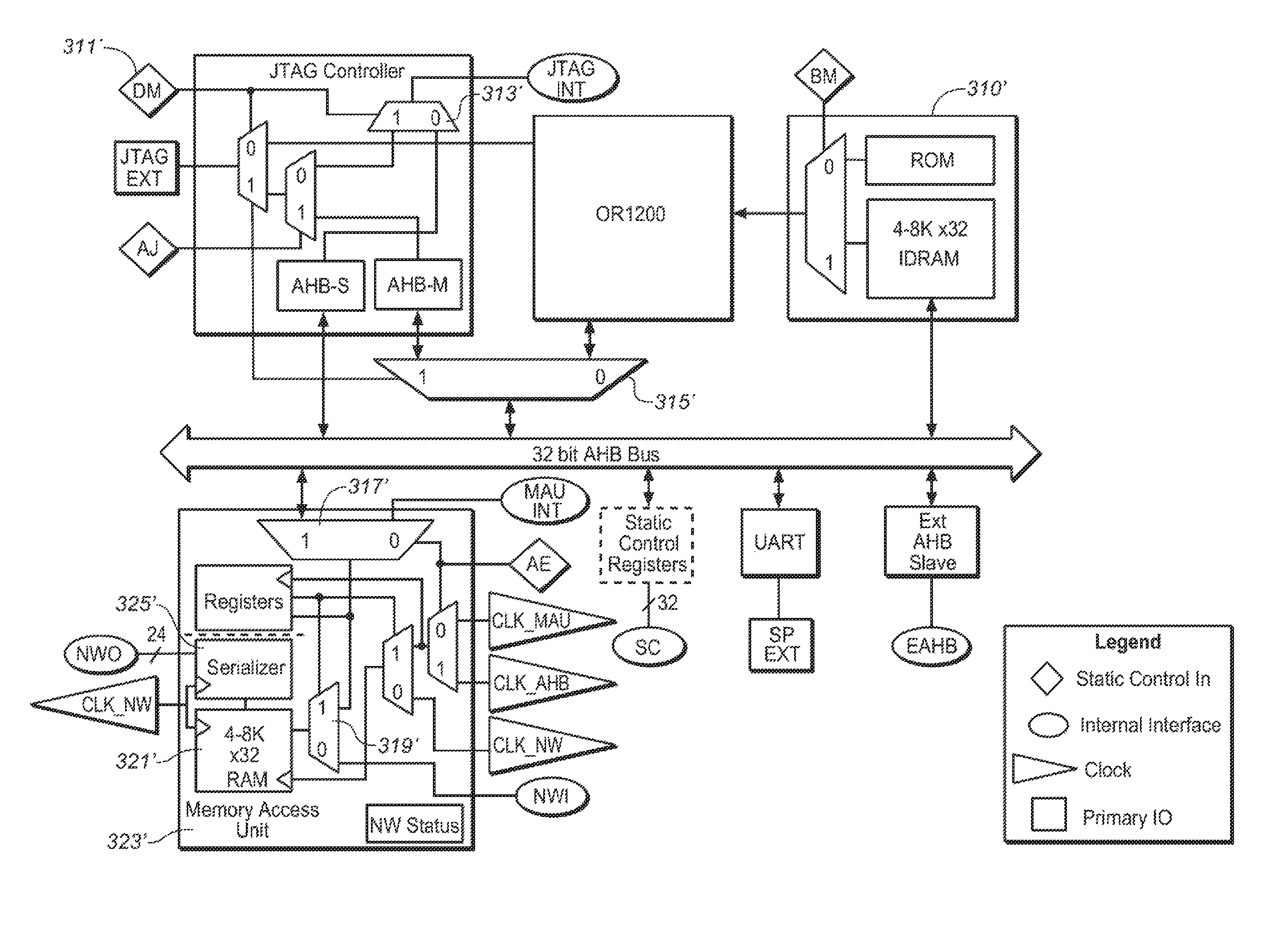
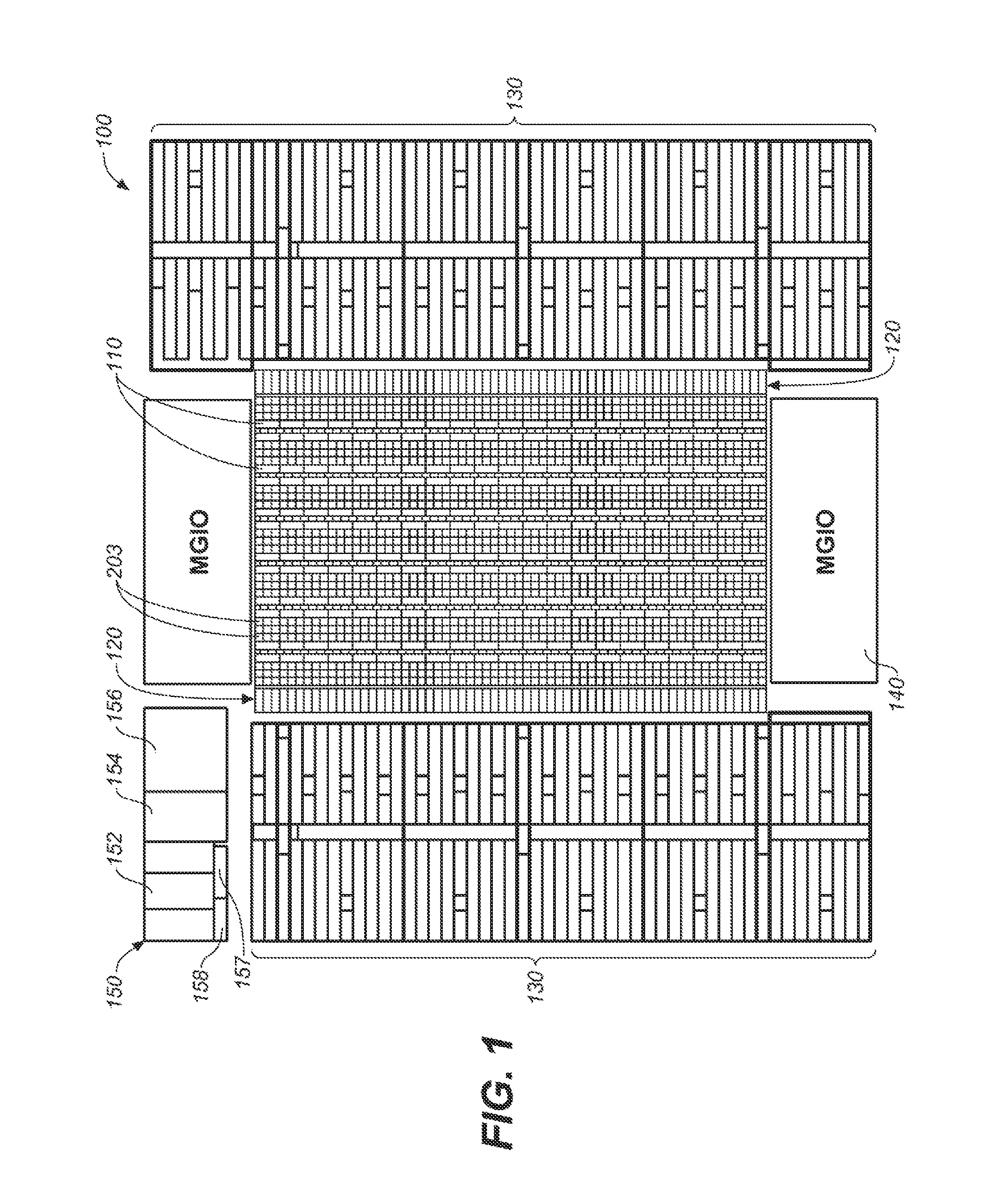
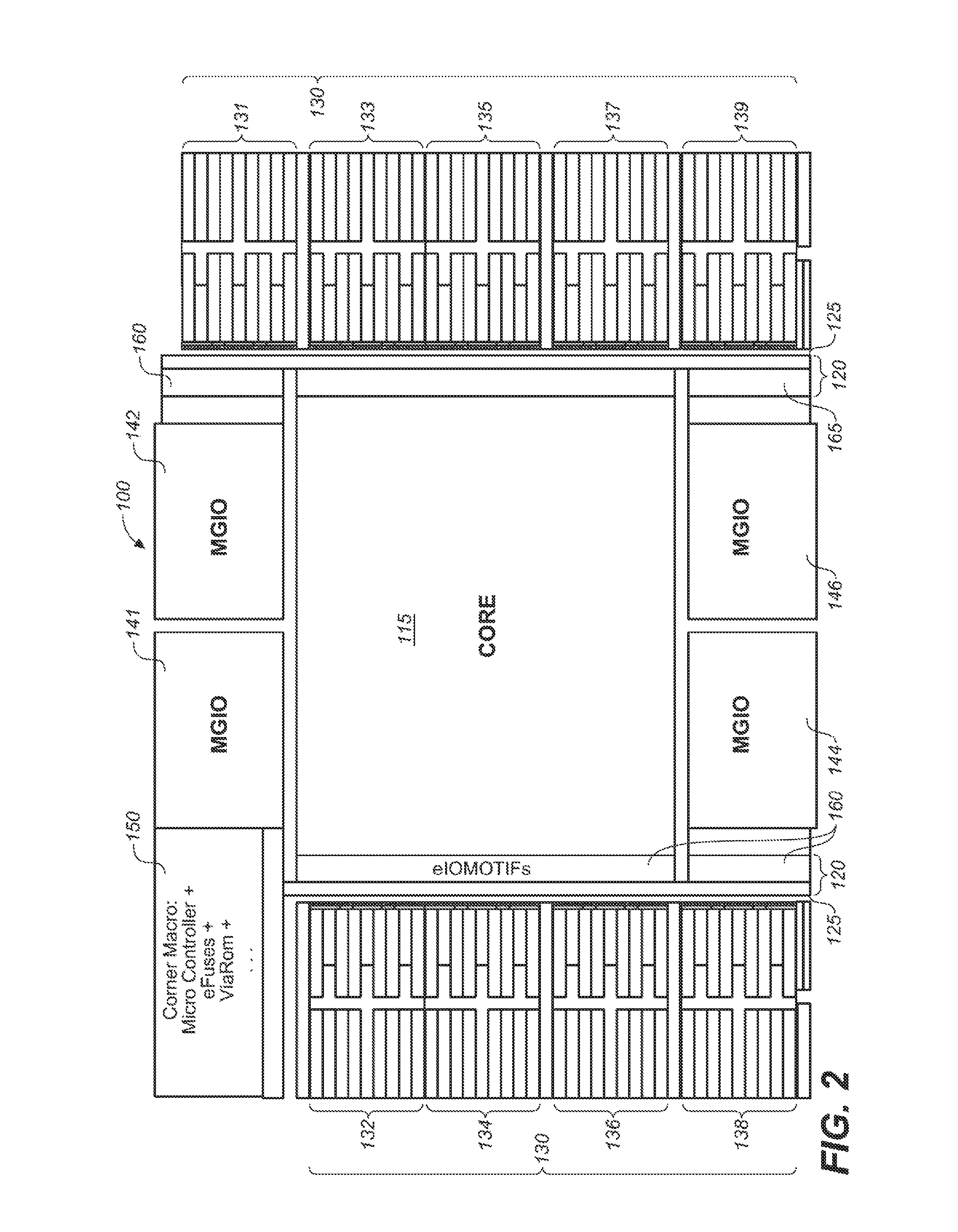
[0064]The method and apparatus of the present invention may be described in software, such as the representation of the invention in an EDA tool, or realized in hardwire, such as the actual physical instantiation.

[0065]Regarding the floorplan of the present invention, the drawings sometimes show elements as blocks that in a physical implementation may differ from this stylized representation, but the essential features of the floorplan should be apparent to one of ordinary skill in the art from the teachings herein.

[0066]The elements in the floor plan of the present invention are operatively connected to one another where necessary, as can be appreciated by one of ordinary skill in the art from the teachings herein. As can be appreciated by one of ordinary skill, a conducting path is operatively connected to another conducting path even though there may be an intervening element between the two paths, such as a register or buffer.

[0067]According to an embodiment of the invention, th...


PUM


Abstract

A network-fabric used for testing with an external or internal tester is shown for a Structured ASIC. In one embodiment, the Structured ASIC uses a microprocessor, network-aware IO routing fabric comprising network agents in a scalable novel configuration, with the network-aware IO having a plurality of blocks connected in series in a plurality of paths in the fabric leading to and from the microprocessor and memory and/or logic, the blocks acting as intelligent network agents under processor control to determine what state they can assume, whether to pass a data signal or not along these paths, comprising open loops and closed loops running to and from the microprocessor and memory and/or logic, primarily for testing and determining the state of the memory and logic. In another embodiment a JTAG controller may receive JTAG test commands from an external testing apparatus and set up to communicate along the fabric.

Description

CROSS-REFERENCE TO RELATED APPLICATIONS[0001]The present application is related to: U.S. application Ser. No. 13 / 649,510, for “VIA-CONFIGURABLE HIGH-PERFORMANCE LOGIC BLOCK INVOLVING TRANSISTOR CHAINS” by Alexander Andreev, Sergey Gribok, Ranko Scepanovic, Phey-Chuin TAN, Chee-Wei KUNG, filed the same day as the present invention, Oct. 11, 2012; U.S. application Ser. No. 13 / 49 529, for “ARCHITECTURAL FLOORPLAN FOR A STRUCTURED ASIC MANUFACTURED ON A 28 NM CMOS PROCESS LITHOGRAPHIC NODE OR SMALLER” by Alexander Andreev, Ranko Scepanovic, Ivan Pavisic, Alexander Yahontov, Mikhail Udovikhin, Igor Vikhliantsev, Chong-Teik LIM, Seow-Sung LEE, Chee-Wei KUNG, filed the same day as the present invention, Oct. 11, 2012; U.S. application Ser. No. 13 / 649,547, for “CLOCK NETWORK FISHBONE ARCHITECTURE FOR A STRUCTURED ASIC MANUFACTURED ON A 28 NM CMOS PROCESS LITHOGRAPHIC NODE” by Alexander Andreev, Andrey Nikishin, Sergey Gribok, Phey-Chuin TAN, Choon-Hun CHOO, filed the same day as the present...

Claims


Application Information

Patent Timeline
Patent Type & Authority Patents(United States)
IPC IPC(8): G06F17/50G06F11/22
CPCG06F11/267G06F17/50G06F11/22
Inventor ANDREEV, ALEXANDERNIKITIN, ANDREYSERBIAN, MARIANVERITA, MASSIMO
Owner INTEL CORP
Why Eureka
Try Eureka