Trench MOSFET with trench contact holes and method for fabricating the same

a technology of trench contact holes and mosfet, which is applied in the direction of basic electric elements, electrical apparatus, and semiconductor devices, can solve the problems of affecting the test performance of the device as well as the production yield, the production process of trench contact holes in the large scale integrated circuit processing production is not suitable, and the solubility of metals and silicon is effectively prevented. , the effect of preventing the breakdown of the junction

Active Publication Date: 2014-04-15
WILL SEMICON (SHANGHAI) CO LTD
View PDF10 Cites 6 Cited by
  • Summary
  • Abstract
  • Description
  • Claims
  • Application Information

AI Technical Summary

Benefits of technology

[0016]The present invention intends to solve the technical problem on how to overcome the defects as follows: the contact holes are not well-filled, voids appear in the trenches and the breakdown of a PN junction easily occurs. To this end, a trench MOSFET device which is suitable for small size contact holes (less than 0.3 um) and a method for fabricating the same are provided.
[0074]2. The mutual solubility between metals and silicon is effectively prevented and the breakdown of the junction is also prevented by using tungsten as a filling material and adding a barrier layer between silicon and tungsten.

Problems solved by technology

However, it also brings new requirements for the manufacturing process of a device: as unit cell pitches are reduced, the controllable range of the diffusion process used during the production of source blocks will become smaller and smaller, and it is likely to cause an imperfect contact between source contact holes and the substrate of a device, which affects the test performance of the device as well as the production yield.
As the trench power MOSFET is of a longitudinal structure, the production process for trench contact holes in the large scale integrated circuit processing production is not suitable for the production methods of contact holes of the trench power MOSFET; meanwhile, there are similar production processes for trench contact holes in the prior art related to trench power MOSFET process, but the production process for the trench power MOSFET with the trench contact holes comprises six photolithographic procedures as blow:
As a result, the trench power MOSFET device may have reliability problems in actual use, which directly affects the application function of the device.
Although the breakdown can be prevented by adding 1% Si into Al, still, Si will readily form Si accumulation in Al which results in larger contact resistance and other adverse effects.
Using source block photolithography to control the spacing between adjacent source blocks has the following defects: in the case of the smaller unit cell, the horizontal diffusion of N+ impurities will be more difficult to control during the thermal process of the production of source blocks, so the ion implantation into the source region is typically replaced by implanting N+ ions into the entire ‘source block island’ surrounded by ‘trenches’.
If the process of contact hole as shown in FIG. 2 is still used, the P well will not be able to contact the source block, which causes undesirable ground connection, and thus deteriorates electric characteristics of the transistor.

Method used


Image

  • Trench MOSFET with trench contact holes and method for fabricating the same
  • Trench MOSFET with trench contact holes and method for fabricating the same
  • Trench MOSFET with trench contact holes and method for fabricating the same

Examples


embodiment 1

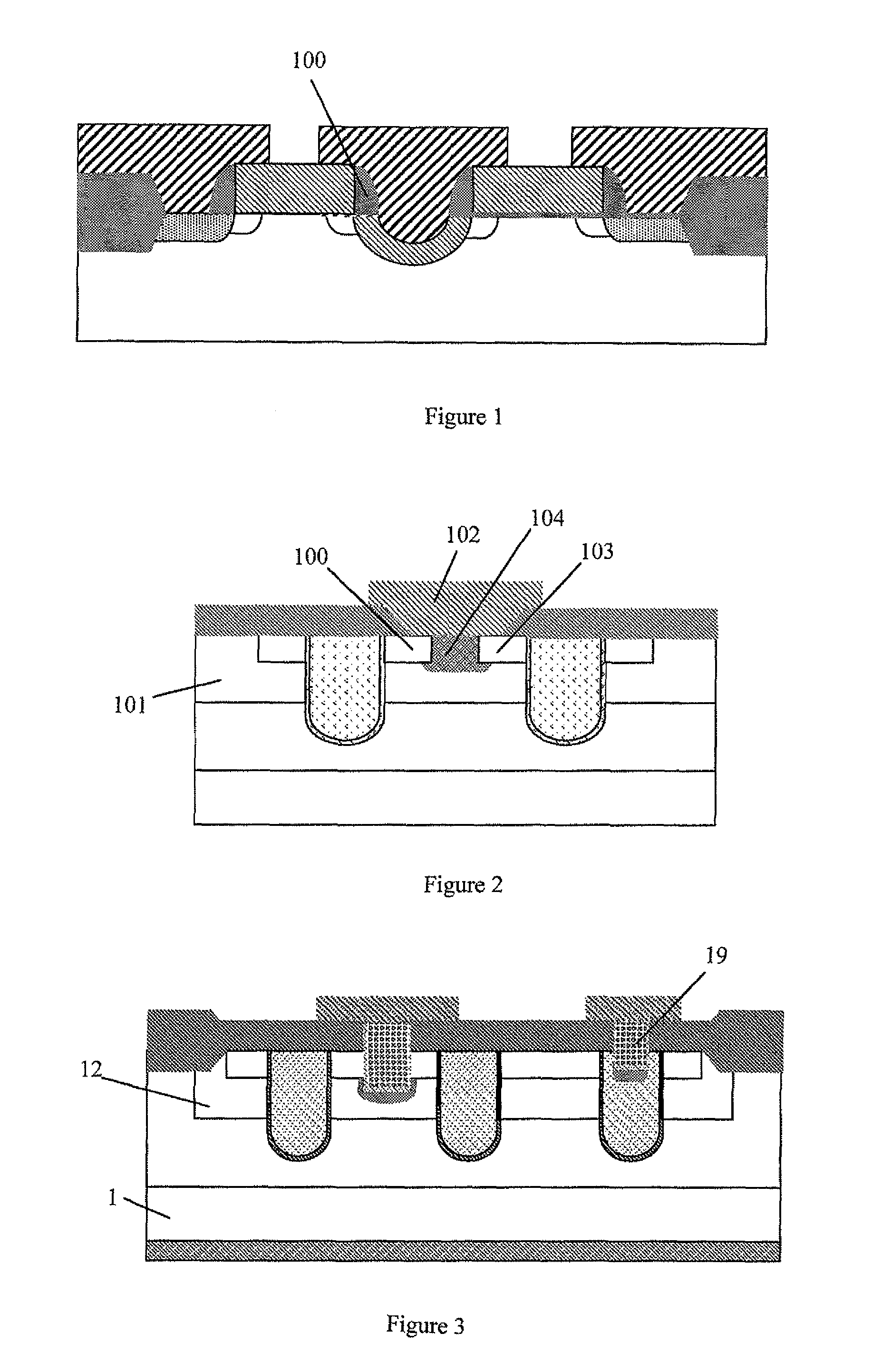
[0080]According to FIGS. 3-15, the detailed embodiment is now given below and numerous specific details are provided to make sure those who skilled in the art will more readily understand the structure features and functional features of the present invention, said detailed description is not to be construed as limiting the invention.

[0081]As shown in FIGS. 4-15, the production of the trench MOSFET in the present invention comprises the following processing steps:

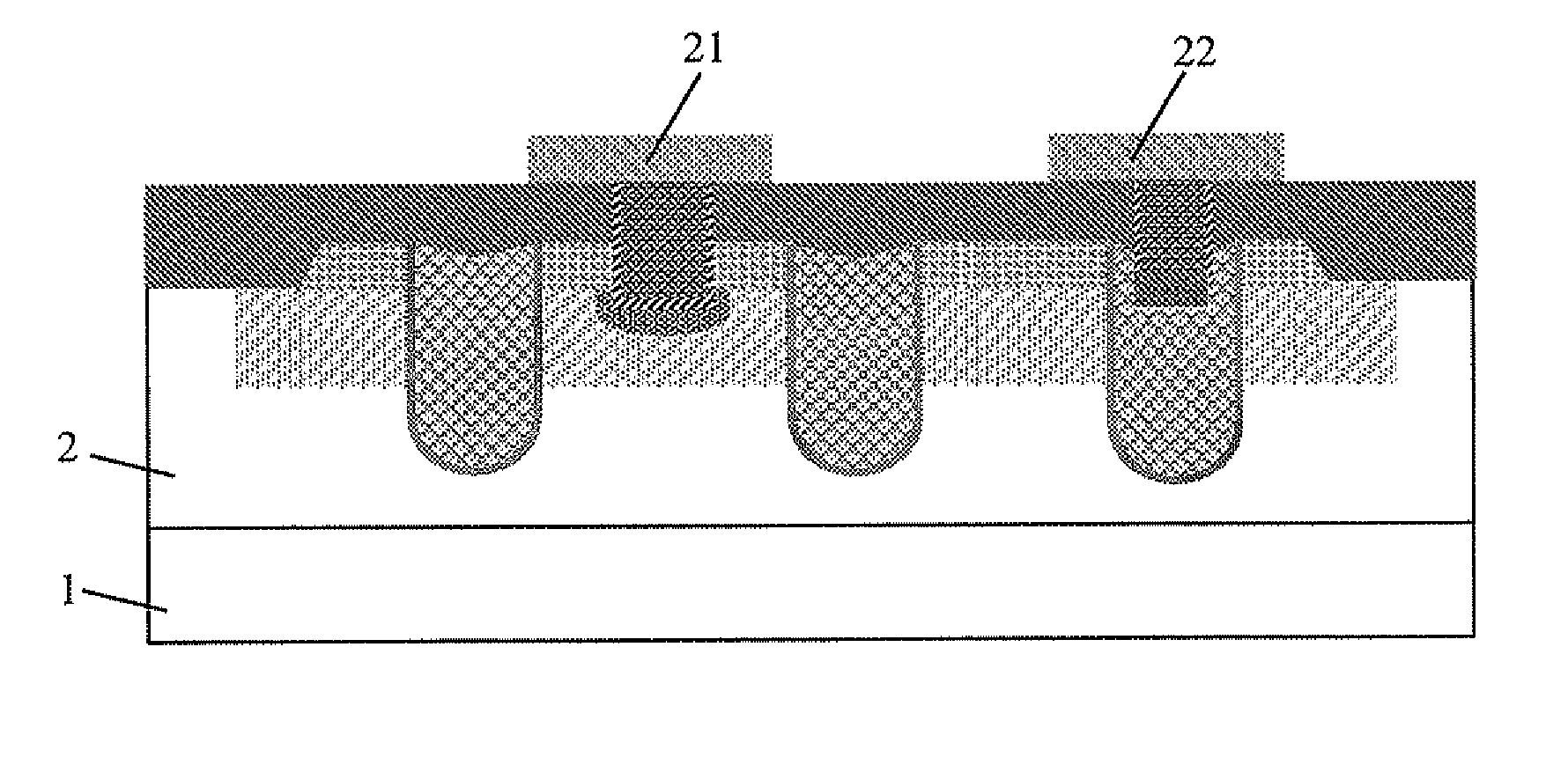
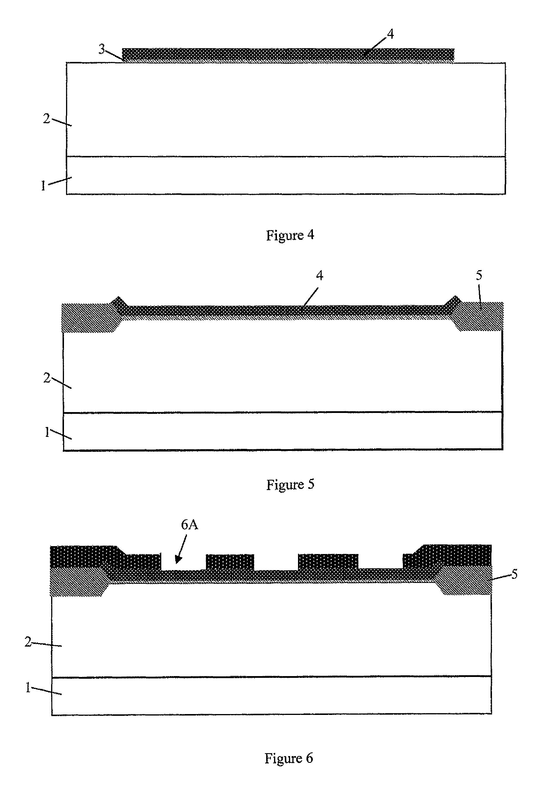
[0082]Step 1: refer to FIG. 4, providing a N type substrate 1 and forming a N type epitaxial layer 2 on the N type substrate 1, wherein the substrate 1 is doped with As ions and said substrate 1 has a electrical resistivity of 0.001-0.002 Ω·cm and a concentration of 3-4e19 / cm3. The epitaxial layer is doped with N− ions and has a thickness of 2.5-3.5 um, the electrical resistivity of said epitaxial layer is 0.2-0.4 Ω·cm, and the concentration of said epitaxial layer is about 1-2e16 / cm3.

[0083]Step 2: refer to FIGS. 4-8, etchi...

embodiment 2

[0107]This embodiment adopts the P-type semiconductor. The principle and processing steps thereof are both the same as Embodiment 1 and the differences are as follows: the substrate adopted is a P-type substrate, the epitaxial layer grown on the substrate is a P-type epitaxial layer, the well on top of the epitaxial layer is a N well region, the source region on the N well region is a P+ type source region, in-situ P+ doped polysilicon is in the trenches, and the implanted region below trench contact holes is a N+ implanted region. Besides, the oxide layer and metals filled in the trench contact holes are all the same as those in Embodiment 1.

[0108]The present invention is based on four steps of etching process, wherein the trench contact hole process is employed to enable the contact holes to traverse the source block and the P well region to reach the substrate region, namely, the drain region, in which way, after the posterior metal process, a desirable contact can be ensured to ...


PUM


Abstract

A trench MOSFET with trench contact holes and a method for fabricating the same are disclosed. The MOSFET includes an N type substrate, an N type epitaxial layer on the substrate; a P well region on top of the epitaxial layer; a source region formed on the P well region; an oxide layer on the source region; a plurality of trenches which traverse the source region and the P well region and contact the epitaxial layer; a gate oxide layer and polysilicon formed in the trenches; a source contact hole and a gate contact hole, wherein the source contact hole and the gate contact hole have a titanium metal layer, a titanium nitride layer, and tungsten metal sequentially, respectively; a P+ implanted region; a source electrode formed above the source contact hole and a gate electrode formed above the gate contact hole.

Description

FIELD OF INVENTION[0001]This invention relates to a trench MOSFET with trench contact holes and a method for fabricating the same.BACKGROUND OF THE INVENTION[0002]The trench power MOSFET (Metal Oxide Semiconductor Field Effect Transistor) is a power semiconductor device of a new generation, which has a fast switching speed, high input resistance and negative temperature coefficient. Compared with the VDMOS (vertical conductiondouble scattering metal oxide semiconductor), the trench power MOSFET can enable chips to be made in smaller size with low RDS(on) ensured; and it is widely used in high-frequency, medium and low power fields, such as electric vehicles, mobile phones, computer power supplies, and other products.[0003]Because of miniaturization trends of modern electronic products, components are required to have smaller physical volumes, that is, package dimensions of devices are getting smaller and smaller. In order to ensure low RDS(on), the new trench MOSFET has used smaller...

Claims


Application Information

Patent Timeline
Patent Type & Authority Patents(United States)
IPC IPC(8): H01L21/336
CPCH01L29/4958H01L29/42372H01L29/66727H01L29/41766H01L29/66734H01L29/456H01L29/7813
Inventor JI, GANGGU, JIANPINGNI, KAIBINZHONG, TIANBING
Owner WILL SEMICON (SHANGHAI) CO LTD
Why Eureka
Try Eureka