Oxide semiconductor device including gate trench and isolation trench

a semiconductor and gate trench technology, applied in the direction of semiconductor devices, electrical devices, transistors, etc., can solve the problems of inadequacies of methods, deterioration of memory retention characteristics, and inability of transistors to function as switching elements, so as to achieve the suppression of short-channel effects, the frequency of refresh operation can be extremely low, and the power consumption can be adequately reduced.

Inactive Publication Date: 2014-07-01
SEMICON ENERGY LAB CO LTD
View PDF153 Cites 13 Cited by
  • Summary
  • Abstract
  • Description
  • Claims
  • Application Information

AI Technical Summary

Benefits of technology

[0015]Therefore, it is an object of one embodiment of the present invention to provide a semiconductor device in which improvement of a property of holding stored data can be achieved. Further, it is an object of one embodiment of the present invention to reduce the power consumption of a semiconductor device. Furthermore, it is an object of one embodiment of the present invention to provide a semiconductor device having a novel structure, which does not have a limitation on the number of write cycles.
[0016]In the disclosed invention, a semiconductor device is formed using a wide-gap semiconductor material capable of sufficiently reducing the off-state current of a transistor (for example, an oxide semiconductor material). The use of a semiconductor material capable of sufficiently reducing the off-state current of a transistor enables data to be held for a long time.
[0028]Since the off-state current of a transistor including a wide-gap semiconductor (for example, an oxide semiconductor) is extremely small, stored data can be held for an extremely long period by using the transistor for a semiconductor memory device. In other words, power consumption can be adequately reduced because refresh operation of a semiconductor memory device becomes unnecessary or the frequency of refresh operation can be extremely low.
[0029]In the transistor having a trench structure disclosed in this specification, the occurrence of a short-channel effect can be suppressed by appropriately setting the depth of the first trench even when the distance between the source electrode and the drain electrode is decreased.

Problems solved by technology

However, in a transistor having a channel length of 100 nm or less, a punch-through current is likely to flow due to a short-channel effect and the transistor becomes incapable of functioning as a switching element, which has been considered to be a problem.
This method makes a junction leakage current likely to flow between a source and the substrate or between a drain and the substrate and eventually causes deterioration of memory retention characteristics.
Therefore, the method is not an appropriate solution to the problem.
However, a conventional DRAM needs to be refreshed at an interval of several tens of milliseconds to hold data, which results in large power consumption.
In addition, a transistor therein is frequently turned on and off; thus, deterioration of the transistor is also a problem.
These problems become significant as the memory capacity increases and transistor miniaturization advances.
However, a gate insulating layer included in a storage element deteriorates by tunneling current generated in writing, so that the storage element stops its function after a predetermined number of writing operations.
However, a complicated peripheral circuit is needed to realize this method.
Moreover, employing such a method does not solve the fundamental problem of lifetime.
In other words, a flash memory is not suitable for applications in which data is frequently rewritten.
Further, it takes a relatively long time to hold or remove charge, so that it is not easy to increase the speed of write and erase operations.

Method used


Image

  • Oxide semiconductor device including gate trench and isolation trench
  • Oxide semiconductor device including gate trench and isolation trench
  • Oxide semiconductor device including gate trench and isolation trench

Examples


embodiment 1

[0048]In this embodiment, a semiconductor device that is one embodiment of the present invention and a manufacturing method thereof are described with reference to FIGS. 1A1 and 1A2; FIGS. 2A1, 2A2, 2B1, and 2B2; FIGS. 3A1, 3A2, 3B1, and 3B2; FIGS. 4A1, 4A2, 4B1, and 4B2; FIGS. 5A1, 5A2, 5B1, and 5B2; FIGS. 6A1, 6A2, 6B1, and 6B2; FIGS. 7A1, 7A2, 7B1, and 7B2; and FIGS. 8A1 and 8A2.

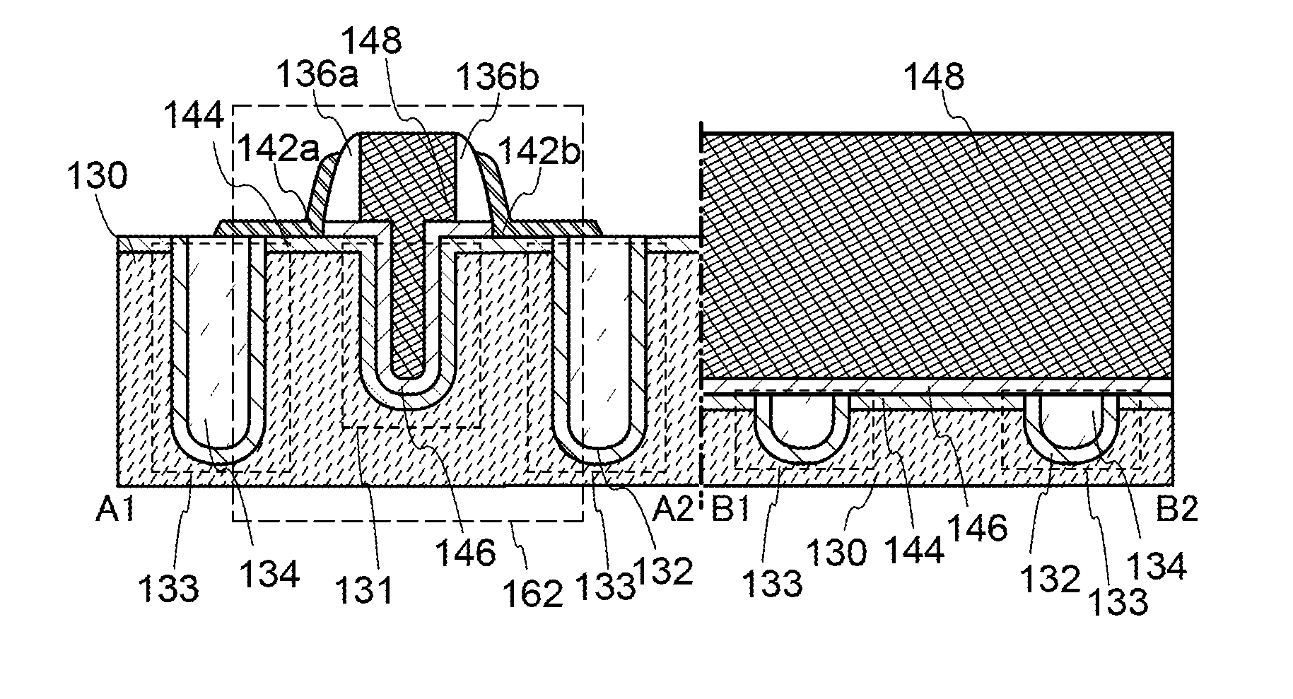
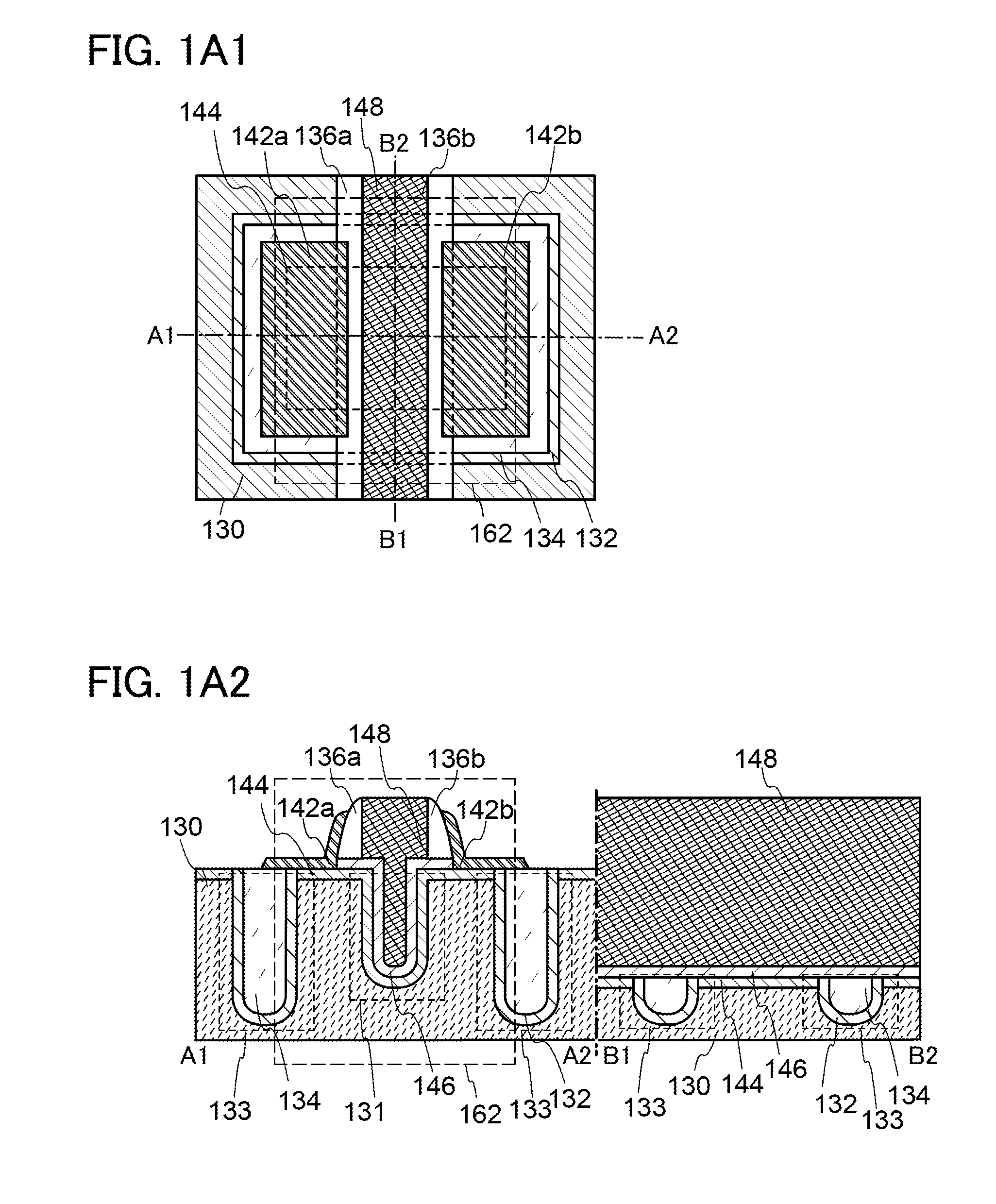
[0049]FIG. 1A1 illustrates an example of a plan view of a transistor 162 in this embodiment. Further, FIG. 1A2 illustrates cross-sections taken along the chain line A1-A2 and the chain line B1-B2 in FIG. 1A1.

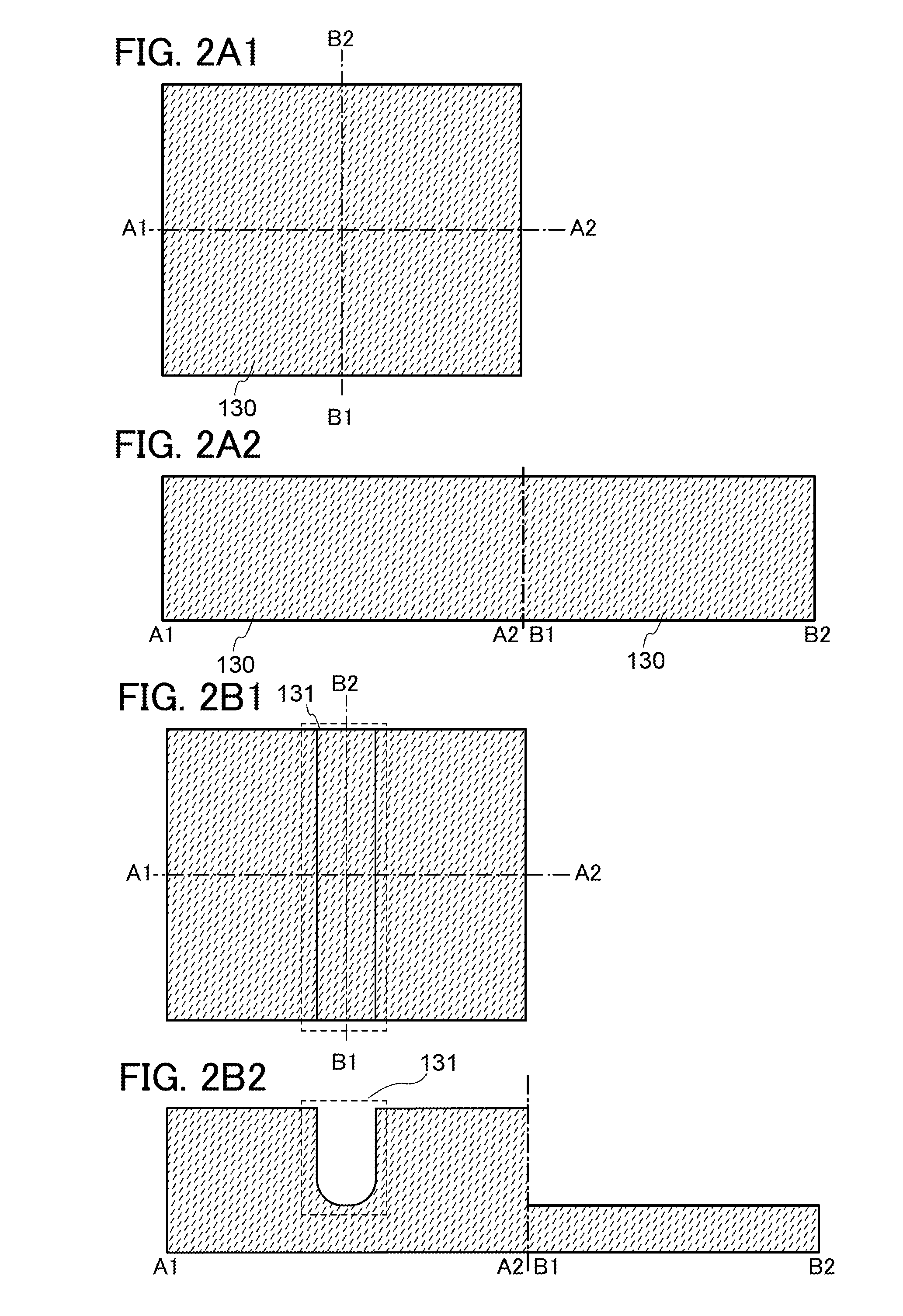
[0050]The transistor 162 described in this embodiment includes an insulating layer 130 in which a first trench 131 and a second trench 133 are provided, an oxide semiconductor layer 144 provided in contact with a bottom surface and an inner wall surface of the first trench 131, an insulating layer 132 provided in contact with a bottom surface and an inner wall surface of the second trench 133, an insu...

embodiment 2

[0111]In this embodiment, an example of a semiconductor device which includes the transistor 162 described in Embodiment 1, which can hold stored data even when not powered, and which does not have a limitation on the number of write cycles, will be described with reference to the drawings.

[0112]Since the off-state current of the transistor 162 is small, stored data can be held for a long time owing to such a transistor. In other words, power consumption can be sufficiently reduced because a semiconductor device in which refresh operation is unnecessary or the frequency of refresh operation is extremely low can be provided.

[0113]FIGS. 9A to 9C illustrate one example of a structure of the semiconductor device. FIGS. 9A to 9C illustrate a cross-sectional view, a plan view, and a circuit diagram, respectively, of the semiconductor device. Here, FIG. 9A corresponds to cross sections taken along the chain line C1-C2, the chain line D1-D2, and the chain line E1-E2 of FIG. 9B.

[0114]The sem...

embodiment 3

[0135]In this embodiment, a semiconductor device which includes the transistor 162 described in Embodiment 1, which can hold stored data even when not powered, which does not have a limitation on the number of write cycles, and which has a structure different from the structure described in Embodiment 2, will be described with reference to FIGS. 10A and 10B and FIGS. 11A and 11B.

[0136]FIG. 10A illustrates an example of a circuit configuration of a semiconductor device, and FIG. 10B is a conceptual diagram illustrating an example of a semiconductor device. First, the semiconductor device illustrated in FIG. 10A will be described, and then, the semiconductor device illustrated in FIG. 10B will be described.

[0137]In the semiconductor device illustrated in FIG. 10A, a bit line BL is electrically connected to a source electrode or a drain electrode of the transistor 162, a word line WL is electrically connected to a gate electrode of the transistor 162, and a source electrode or a drain ...


PUM


Abstract

A semiconductor device in which improvement of a property of holding stored data can be achieved. Further, power consumption of a semiconductor device is reduced. A transistor in which a wide-gap semiconductor material capable of sufficiently reducing the off-state current of a transistor (e.g., an oxide semiconductor material) in a channel formation region is used and which has a trench structure, i.e., a trench for a gate electrode and a trench for element isolation, is provided. The use of a semiconductor material capable of sufficiently reducing the off-state current of a transistor enables data to be held for a long time. Further, since the transistor has the trench for a gate electrode, the occurrence of a short-channel effect can be suppressed by appropriately setting the depth of the trench even when the distance between the source electrode and the drain electrode is decreased.

Description

BACKGROUND OF THE INVENTION[0001]1. Field of the Invention[0002]The invention disclosed in this specification relates to a semiconductor device using a semiconductor element.[0003]2. Description of the Related Art[0004]Storage devices using semiconductor elements are broadly classified into two categories: a volatile device that loses stored data when power supply stops, and a non-volatile device that retains stored data even when power is not supplied.[0005]A typical example of a volatile storage device is a DRAM (dynamic random access memory). A memory cell which is a key component in a DRAM includes a read and write transistor and a capacitor.[0006]Circuit patterns for DRAMs, like those for other semiconductor integrated circuits, have been increasingly miniaturized in accordance with the scaling law. However, in a transistor having a channel length of 100 nm or less, a punch-through current is likely to flow due to a short-channel effect and the transistor becomes incapable of f...

Claims


Application Information

Patent Timeline
Patent Type & Authority Patents(United States)
IPC IPC(8): H01L29/786
CPCH01L27/1156H01L21/76232H01L27/1225H01L29/4236H10B41/70
Inventor ISOBE, ATSUOSAITO, TOSHIHIKOKATO, KIYOSHI
Owner SEMICON ENERGY LAB CO LTD
Why Eureka
Try Eureka