
Nickel thin film, method for formation of the nickel thin film, ferromagnetic nano-junction element, method for producing the ferromagnetic nano-junction element, thin metallic wire, and method for formation of the thin metallic wire

a nickel thin film and nano-junction technology, applied in the field of nickel thin film, can solve the problems of difficult to completely remove roughness on the surface of a substrate made of organic materials, and difficult to form metal thin films, and achieve the effects of small surface roughness, small surface roughness, and small surface roughness

Inactive Publication Date: 2014-08-05
HOKKAIDO UNIVERSITY
View PDF7 Cites 5 Cited by
  • Summary
  • Abstract
  • Description
  • Claims
  • Application Information

AI Technical Summary

Benefits of technology

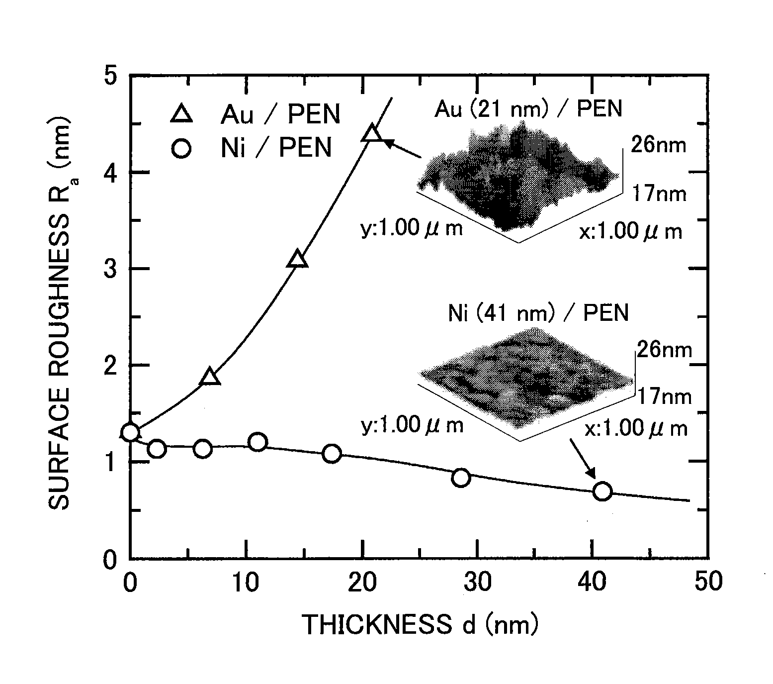
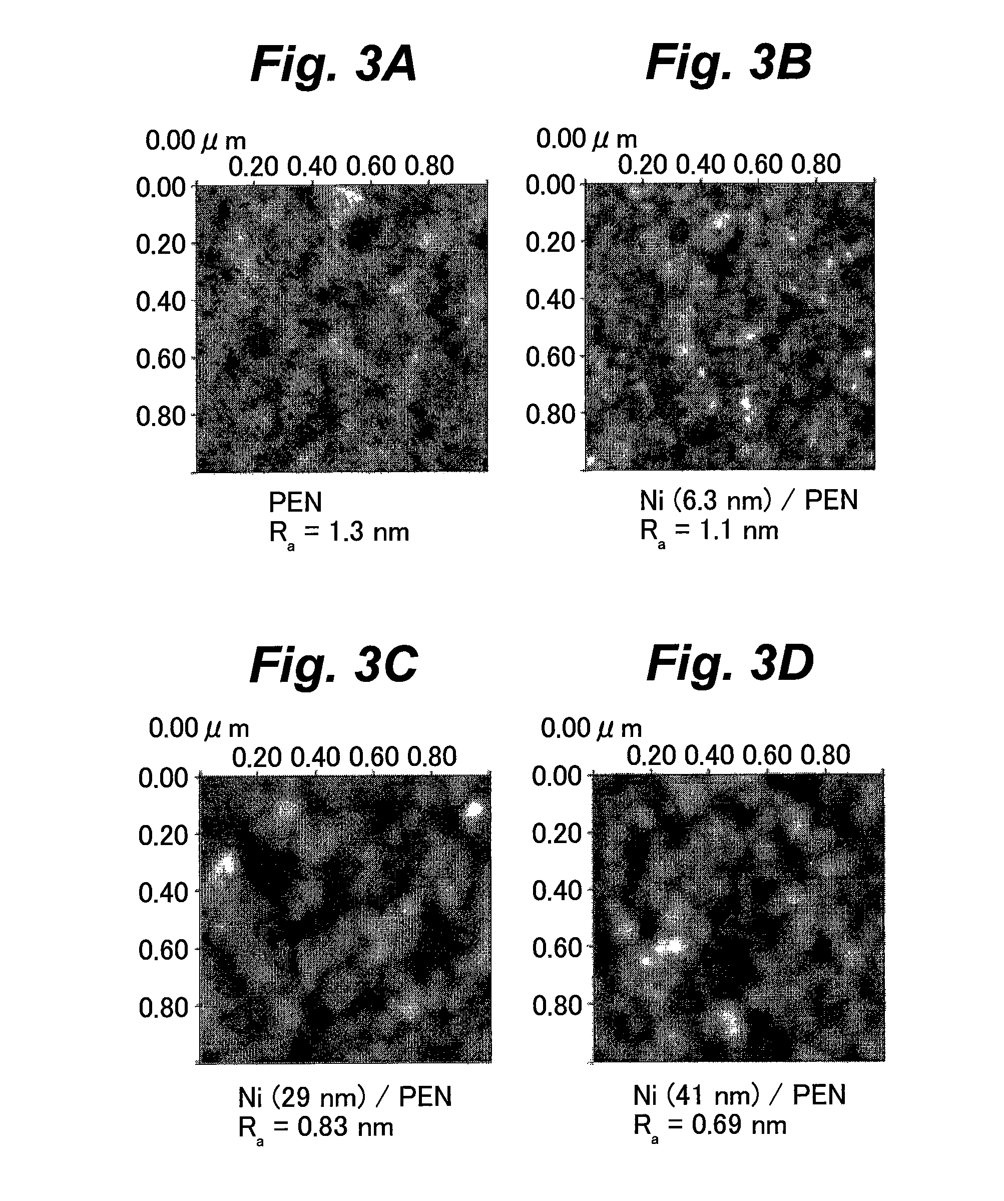
The invention relates to a method for making a thin film with ultra-high surface smoothness and atomic-level flatness. The method can be used to create a thin metallic wire and a ferromagnetic nano-junction element with a giant magnetoresistance effect. By using a polyethylene naphthalate substrate with a very smooth surface and a vacuum evaporation method for film formation, a nickel thin film can be obtained with surface roughness of 1 nm or less. A thicker nickel thin film can further decrease surface roughness and obtain a more atomic-level flat surface. The thickness of the nickel thin film can be appropriately controlled by controlling the temperature and speed of film formation. The invention also includes a method of joining two laminates with nanometer-order thick nickel thin films to create a ferromagnetic nano-junction element showing a giant magnetoresistance effect at room temperature.

Problems solved by technology

However, it is very difficult to completely remove roughness on a surface of a substrate made of organic material.
Therefore, it is difficult to form a metal thin film having an atomic scale flat surface on a substrate made of organic material so far.

Method used


Image

  • Nickel thin film, method for formation of the nickel thin film, ferromagnetic nano-junction element, method for producing the ferromagnetic nano-junction element, thin metallic wire, and method for formation of the thin metallic wire
  • Nickel thin film, method for formation of the nickel thin film, ferromagnetic nano-junction element, method for producing the ferromagnetic nano-junction element, thin metallic wire, and method for formation of the thin metallic wire
  • Nickel thin film, method for formation of the nickel thin film, ferromagnetic nano-junction element, method for producing the ferromagnetic nano-junction element, thin metallic wire, and method for formation of the thin metallic wire

Examples


first embodiment

[0039]First, a method for formation of a nickel thin film according to the present invention is explained.

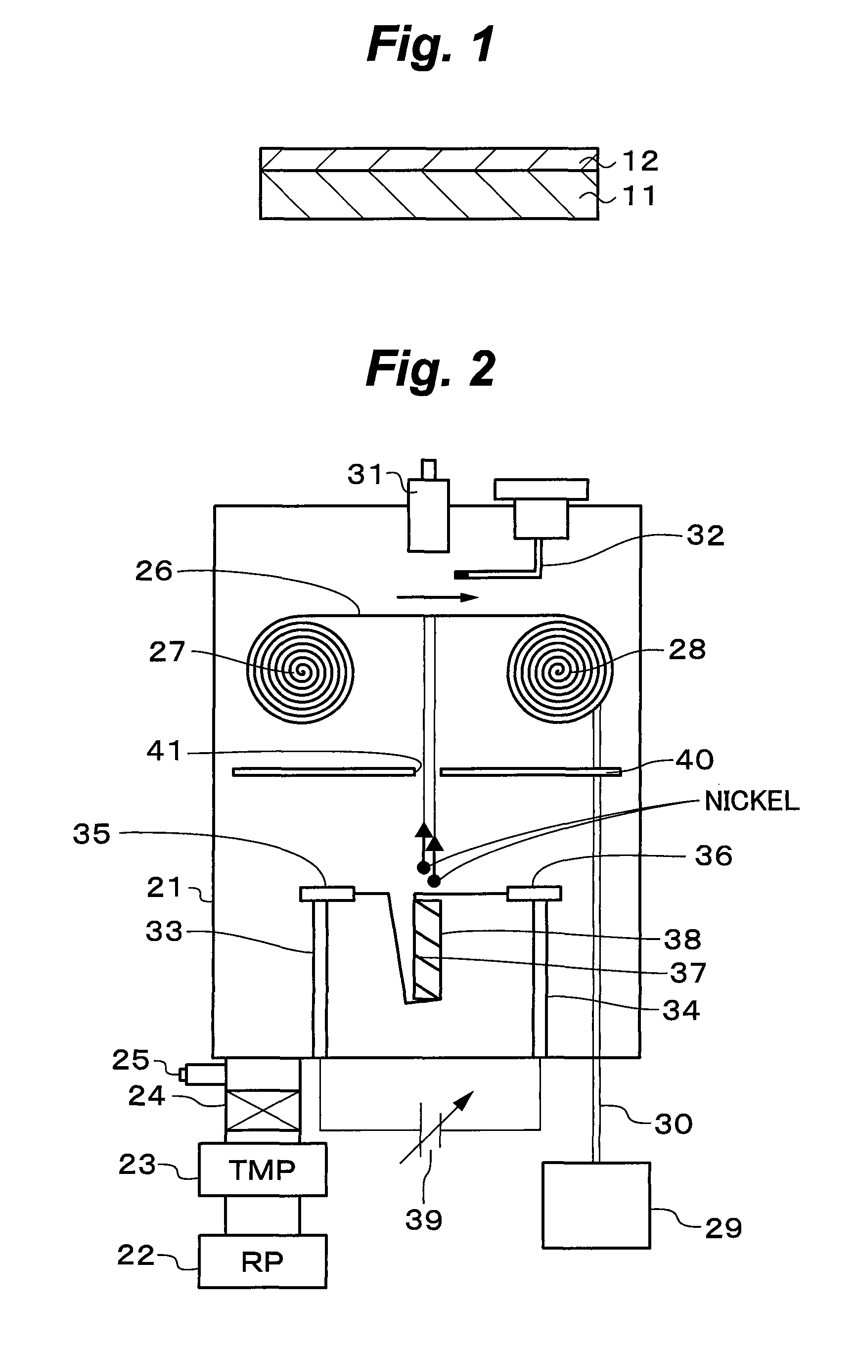
[0040]As shown in FIG. 1, in a method for formation of a nickel thin film, a nickel thin film 12 is formed on a polyethylene naphthalate substrate 11. The configuration of the polyethylene naphthalate substrate 11 is not limited, and it may be a film-like substrate, a sheet-like substrate or a bulk substrate. The vacuum evaporation method, etc. is used to form the nickel thin film 12. The temperature to form the film is, for example, room temperature.

[0041]An example is explained.

[0042]As the polyethylene naphthalate substrate 11, a PEN film (trade name: TEONEX Q65) having 5 mm width and 100 μm thickness supplied by Teijin DuPont Japan Ltd. is cut down to 2 mm width by using a slitter with the film-rolling-up system in clean environment. On the PEN film having 2 mm width and 100 μm thickness prepared by the above process, a nickel thin film 12 is formed by a vacuum evaporation m...

second embodiment

[0057]Next, a magnetoresistance effect element according to the present invention is explained. The magnetoresistance effect element is made using the ferromagnetic nano-junction of nickel thin films.

[0058]FIG. 8 shows the magnetoresistance effect element. As shown in FIG. 8, the magnetoresistance effect element is made by using two laminates each comprising the nickel thin film 12 formed on the polyethylene naphthalate substrate 11 by the same method of the first embodiment, and joining these two laminates so that the nickel thin films 12 cross to each other in such a manner that edges of these nickel thin films 12 face each other. The thickness of the nickel thin film 12 is nanometer order, preferably from one atomic layer to 10 nm. The crossing angle is 90°, for example. FIG. 9 shows the ferromagnetic nano-junction formed by joining the edges of the nickel thin films 12 each other at the cross point. In FIG. 9, the polyethylene naphthalate substrate 11 is not illustrated. In FIG....

third embodiment

[0063]Next, a method for formation of a thin metallic wire according to the present invention is explained.

[0064]According to the third embodiment, by making oblique evaporation using nickel beams by the vacuum evaporator shown in FIG. 2, a nickel thin film 12 is formed on a polyethylene naphthalate substrate 11 as shown in FIG. 1. In the oblique evaporation, the inclination of nickel beams for the major surface of the polyethylene naphthalate substrate 11 is 1 to 3°, for example.

[0065]An example is explained.

[0066]As the polyethylene naphthalate substrate 11, a PEN film (trade name: TEONEX Q65) having 5 mm width and 100 μm thick made by Teijin DuPont Japan Ltd. is used after cutting out in the predetermined shape. The nickel thin film 12 is formed on the PEN film by the oblique evaporation using nickel beams with the inclination of 1 to 3° at room temperature.

[0067]FIG. 12 shows a cross-sectional transmission electron microscope image (cross-sectional TEM image) of a sample formed ...


PUM

PropertyMeasurementUnit
surface roughnessaaaaaaaaaa
thicknessaaaaaaaaaa
thicknessaaaaaaaaaa

Abstract

A nickel thin film is formed, for example, to a thickness of 2 nm or more on a polyethylene naphthalate substrate by a vacuum evaporation method. A magnetoresistance effect element using ferromagnetic nano-junction is comprised by using two laminates each comprising a nickel thin film formed on a polyethylene naphthalate substrate, and joining these two laminates so that the nickel thin films cross to each other in such a manner that edges of the nickel thin films face each other.

Description

CROSS-REFERENCE TO RELATED APPLICATIONS[0001]This application is filed under the provisions of 35 U.S.C. §371 and claims the priority of International Patent Application PCT / JP2008 / 065924 filed on Aug. 28, 2008, which claims priority from Japanese Patent Application No. 248809 / 2007 filed on Sep. 26, 2007, and Japanese Patent Application No. 066929 / 2008 filed on Mar. 17, 2008, all three of which are incorporated by reference herein in their entirety.TECHNICAL FIELD[0002]The present invention generally relates to a nickel thin film, a method for formation of the nickel thin film, a ferromagnetic nano-junction element, a method for producing the ferromagnetic nano-junction element, a thin metallic wire, and a method for formation of the thin metallic wire, which is suitable to apply to a magnetoresistance effect element using ferromagnetic nano-junction, for example.BACKGROUND ART[0003]Conventionally, as methods for formation of an atomic-scale flat surface on a surface of a metallic s...

Claims


Application Information

Patent Timeline
Patent Type & Authority Patents(United States)
IPC IPC(8): H01L43/08C23C14/20H01L43/12C23C14/26H01F41/20H01F10/14B32B15/08C23C16/00
CPCC23C14/20H01L43/12H01L43/08C23C14/26H01F41/20H01F10/14Y10T428/31692Y10T428/2958Y10T428/24942Y10T428/1114H01F10/265Y10T428/12569Y10T428/32H10N50/10H10N50/01
Inventor KAIJU, HIDEOISHIMARU, MANABUHIROTSU, YOSHIHIKOONO, AKITOISHIBASHI, AKIRA
Owner HOKKAIDO UNIVERSITY
Learn More