RF and milimeter-wave high-power semiconductor device

a technology of semiconductor devices and milimeter-waves, applied in semiconductor devices, semiconductor/solid-state device details, electrical apparatus, etc., can solve the problems of heat extraction, heat extraction and microwave performance and device cost are generally difficult to satisfy, flip-chip technology has one main disadvantage, etc., to achieve simple processing of chips and secondary substrates and reduce costs

a technology of semiconductor devices and milimeter-waves, applied in semiconductor devices, semiconductor/solid-state device details, electrical apparatus, etc., can solve the problems of heat extraction, heat extraction and microwave performance and device cost are generally difficult to satisfy, flip-chip technology has one main disadvantage, etc., to achieve simple processing of chips and secondary substrates and reduce costs

US8796843B1Active Publication Date: 2014-08-05GROUP4 LABS

Image

  • RF and milimeter-wave high-power semiconductor device
  • RF and milimeter-wave high-power semiconductor device
  • RF and milimeter-wave high-power semiconductor device

Examples


Embodiment Construction

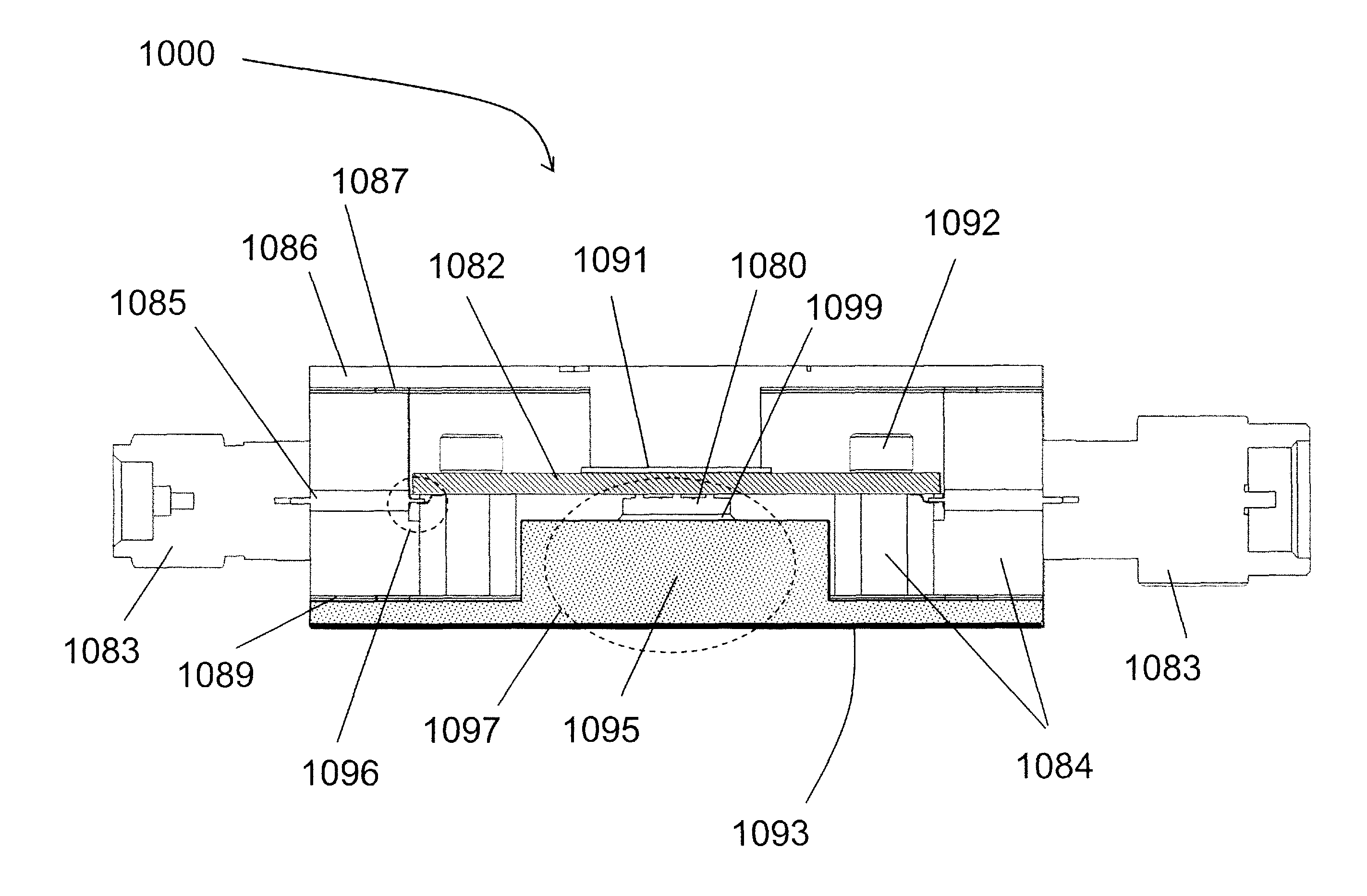
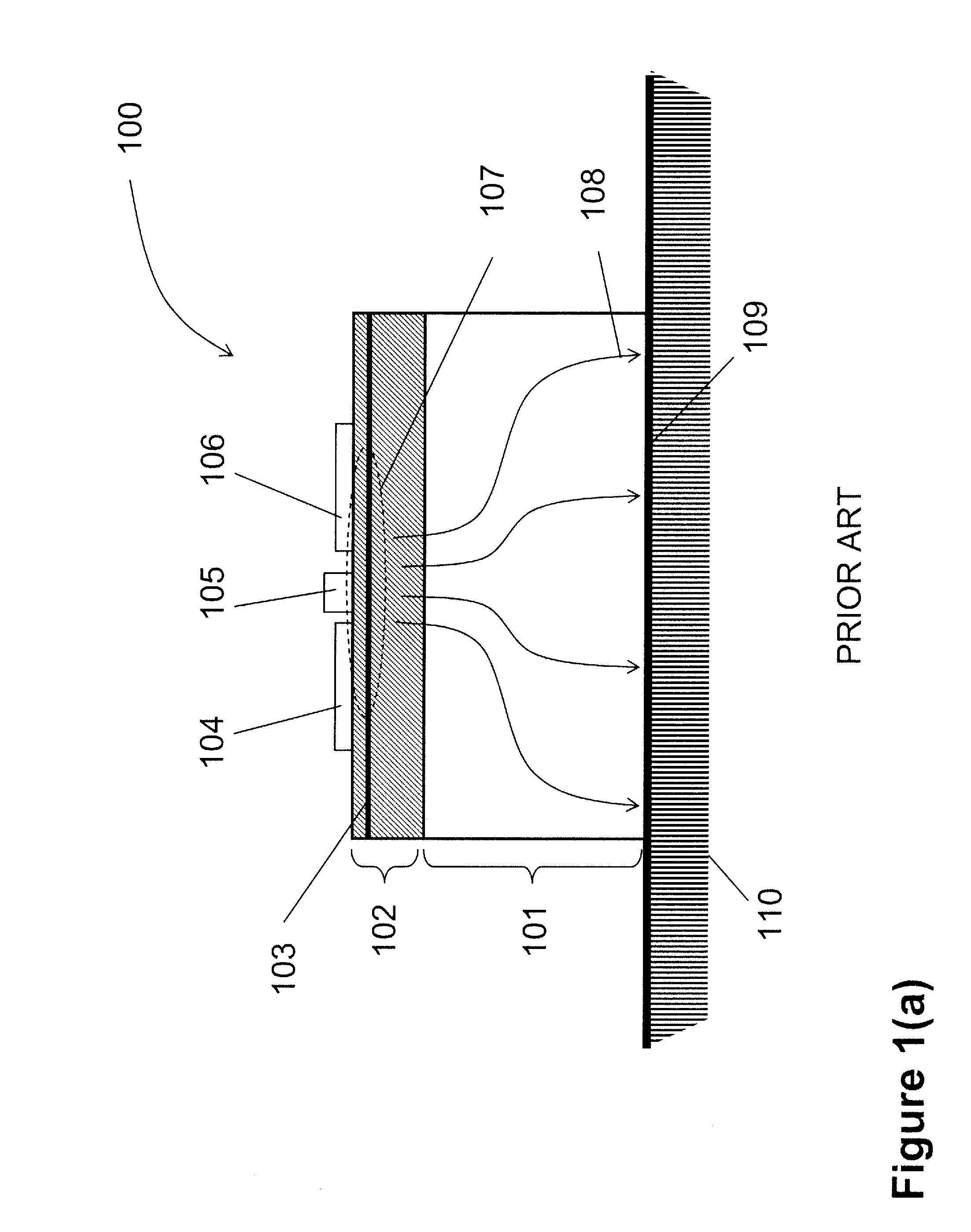
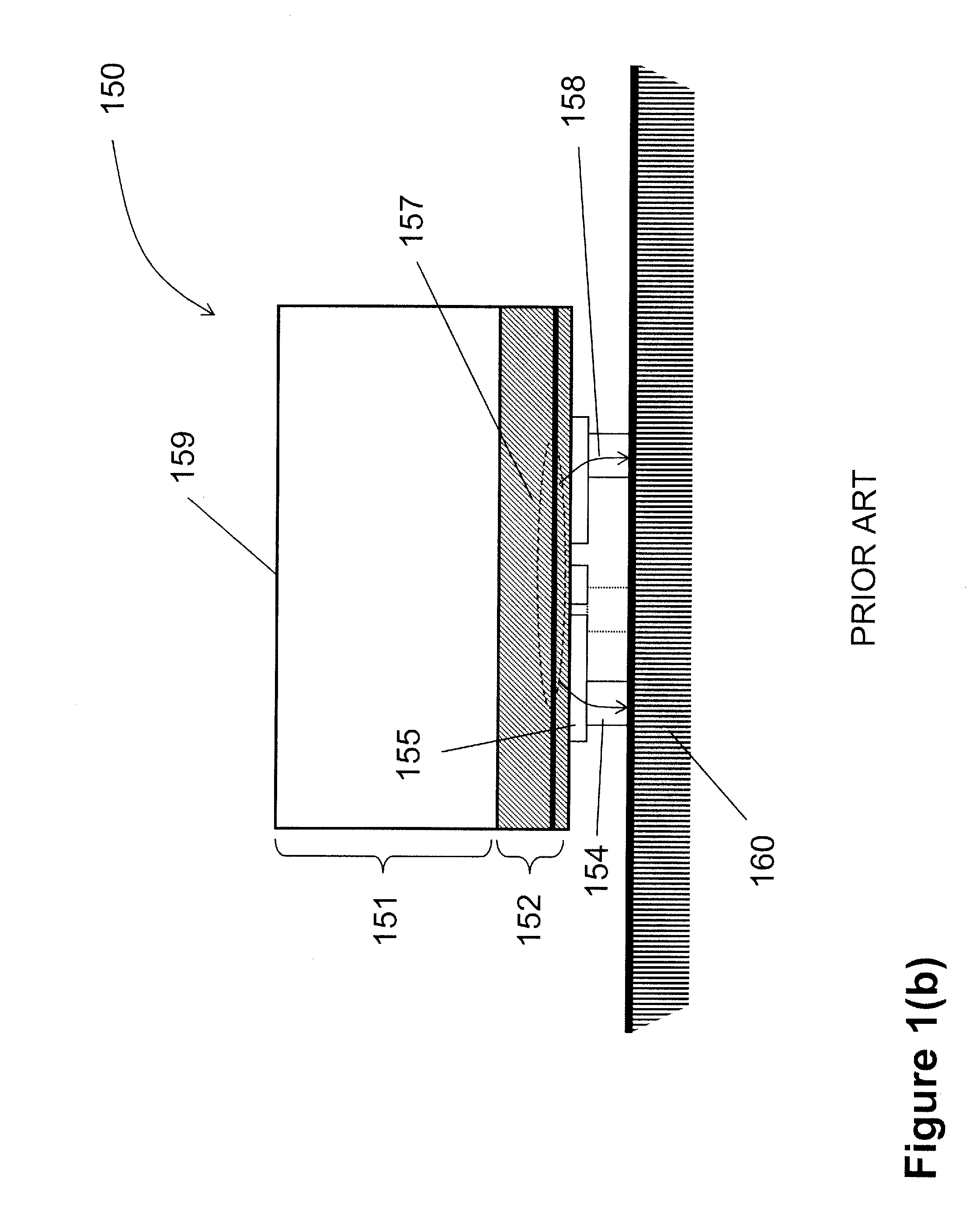
[0073]A discrete field-effect transistor has three terminals: source, gate, and drain terminals. To produce higher power, field-effect transistor are built in parallel so they utilize multiple gates and share multiple drains and sources. The maximum handling power of a field-effect transistor is determined by the maximum current carrying capacity (IDSS) of the channel with the 2D electron gas and the breakdown voltage (VBDS). As the current-carrying capacity (and hence power handling) capacity limited by material and epilayer structure properties, the power handling capacity is largely controlled by increasing the gate periphery (and the width or periphery the associated source and drain periphery that is adjacent to the gate). Due to the resistance of the metallization used to make the gate and resulting phase delay along the gate finger, the gate finger length cannot be increased indefinitely without producing a severe impact on the maximum operating frequency of the transistor. F...


PUM


Abstract

High-power and high-frequency semiconductor devices require high signal integrity and high thermal conductance assembly technologies and packages. In particular, wide-gap-semiconductor devices on diamond benefit from spatially separate electrical and thermal connections. This application discloses assembly and package architectures that offer high signal integrity and high thermal conductance.

Description

RELATED APPLICATIONS[0001]This application claims priority to U.S. Provisional Patent Application Ser. No. 61 / 233,390 filed Aug. 12, 2009.FIELD OF THE INVENTION[0002]The present invention relates to packaging designs and assembly methods for high-power electronic and optoelectronic devices that offer improved thermal management and signal integrity at high frequencies. More specifically, the invention it discloses apparatus embodiments including flip-chip electrical interconnections and heat extraction package designs for gallium-nitride-based devices fabricated on diamond substrates or films. The disclosed embodiments are applicable to wide-gap semiconductor devices fabricated on highly-thermally conductive substrates in general with application in radio-frequency (RF) electronics and optoelectronics.BACKGROUND[0003]Thermal management in semiconductor devices and circuits is a critical design element in any manufacturable and cost-effective electronic and optoelectronic product, su...

Claims


Application Information

Patent Timeline
05 Aug 2014
Publication
US8796843B1
IPC
H01L23/34; H01L23/48
CPC
H01L2224/16225; H01L2224/48465; H01L24/17; H01L2224/48091; H01L2224/73265; H01L2224/10165; H01L23/34; H01L2224/8114
Inventors
BABIC, DUBRAVKO I.; DIDUCK, QUENTIN E.