Semiconductor structure for a radiation detector and a radiation detector

a radiation detector and semiconductor structure technology, applied in the direction of radiation control devices, semiconductor devices, electrical apparatus, etc., can solve the problems of limited function to rather small pixel geometries, significant yield loss, and low resistance semiconductor layers to be used, so as to reduce the so-called “afterpulse” and achieve precise manufacturing of operating point and yield. , the effect of quantum yield

Inactive Publication Date: 2014-09-02
PIERSCHEL MICHAEL
View PDF5 Cites 5 Cited by
  • Summary
  • Abstract
  • Description
  • Claims
  • Application Information

AI Technical Summary

Benefits of technology

[0011]A semiconductor structure for a radiation detector, as well as a radiation detector based hereon, which avoid the disadvantages in prior art is provided. In particular, to enable the manufacture of larger pixel structures for the radiation detector with a better quantum yield, as well as the reduction in so-called “afterpulsing” over larger gap regions. In addition, to support a more precise manufacturing of the operating point and yield.
[0021]In comparison to prior art, it is here proposed that a high-resistance semiconductor substrate be used in place of the low-resistance one. In order to produce the high resistance, the semiconductor substrate (high-resistance semiconductor substrate) can exhibit a specific resistance (specific volume resistance) of at least 300 Ohm cm. Preferably, there is a specific resistance of at least 500 Ohm cm. The transition to intrinsic electrical conduction of the substrate material may provide an upper limit of high resistance.
[0022]Aside from the above, one or more additional doping regions are provided in the semiconductor substrate to go along with the usual doping regions. They form additional doping zones in the semiconductor substrate, and make it possible to provide functions of the previously low-resistance semiconductor substrate. In particular, a precise adjustment of the operating point is supported. The at least one additional doping region, which is allocated to one or more of the doping regions, is used for decoupling from the construction of charge carrier depletion zones required in the overall semiconductor structure, and from the adjustment of the barrier heights required for operation. The provision of one or more additional doping regions yields an additional degree of freedom when designing the semiconductor structure, so that operating points can also be set here, for example, to offset layer thickness fluctuations of used epitaxial substrates.
[0030]One or more additional upper doping regions may be formed in an area of the semiconductor substrate between the cover layer and the doping regions, and the one or more additional upper doping regions may limit avalanche area away from the cover layer toward the doping regions in the semiconductor substrate. By the one or more additional upper doping regions the extension of the avalanche area away from the cover layer toward the doping regions may be limited in the semiconductor substrate. The avalanche area establishes a reproduction region, in which free charge carriers reproduce as the result of collisions after the incident light to be detected has been absorbed. This takes place in the high field strength area (high field). The one or more additional upper doping regions may help make it possible to individually configure the avalanche area.
[0031]One or more additional lower doping regions may be formed in an area of the semiconductor substrate between the substrate and the doping regions, and the one or more additional lower doping regions may limit the extension of the quenching area away from the doping regions toward the substrate in the semiconductor substrate. By the one or more additional lower doping regions the extension of the quenching area away from the doping regions toward the substrate may be limited in the semiconductor substrate. The quenching area is used to again quench the avalanche effect that had previously taken place, so as to quickly enable the detection of subsequent photons (“quenching”). The one or more additional lower doping regions may be used to individually configure the quenching area in the semiconductor substrate.

Problems solved by technology

The main disadvantage to this solution is that rather low-resistance semiconductor layers must be used to ensure reliable function and find a suitable operating point.
In addition, the geometric dimensions and layer thickness of the semiconductor substrate must be precisely adjusted, since the functional limitations associated with the low resistance here yield quite a narrow technological window.
In the typical, unavoidable fluctuations in epitaxial layer thickness from the center to edge of a wafer, this leads to significant losses in yield.
In addition, the fact that a low-resistance substrate material was used directly implies a limitation of function to rather small pixel geometries.
The large capacities of the “floating” structures directly associated therewith greatly limit the potential swing required for function.
This makes it harder to find a suitable operating point for such structures.
In addition, the limitation to very small pixels combined with the density required for the latter to ensure good quantum yield makes so-called “afterpulsing” into a major problem.
If only structures with a pixel geometry of up to roughly 4 micrometers can be realized with the low-resistance substrates, and the gap regions between two pixels are designed to be rather small, so as to achieve good quantum yield, triggering directly adjacent pixels becomes a major problem in such structures, since these kinds of phenomena disrupt the actual measurements.
This design dilemma is directly associated with the use of low-resistance semiconductor layers.

Method used


Image

  • Semiconductor structure for a radiation detector and a radiation detector
  • Semiconductor structure for a radiation detector and a radiation detector
  • Semiconductor structure for a radiation detector and a radiation detector

Examples


Embodiment Construction

[0047]One exemplary embodiment proceeds from an n-conductivity type of material for a semiconductor substrate. However, the aspects of the disclosure can also be applied without limitation to p-conductivity type substrates. In this case, the indicated conductivity types must be cyclically switched.

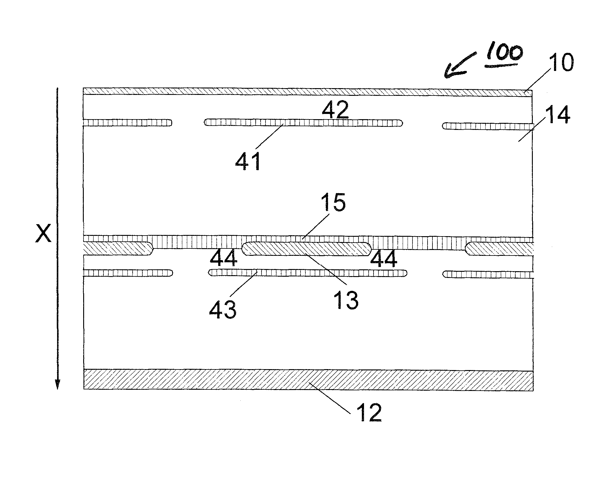
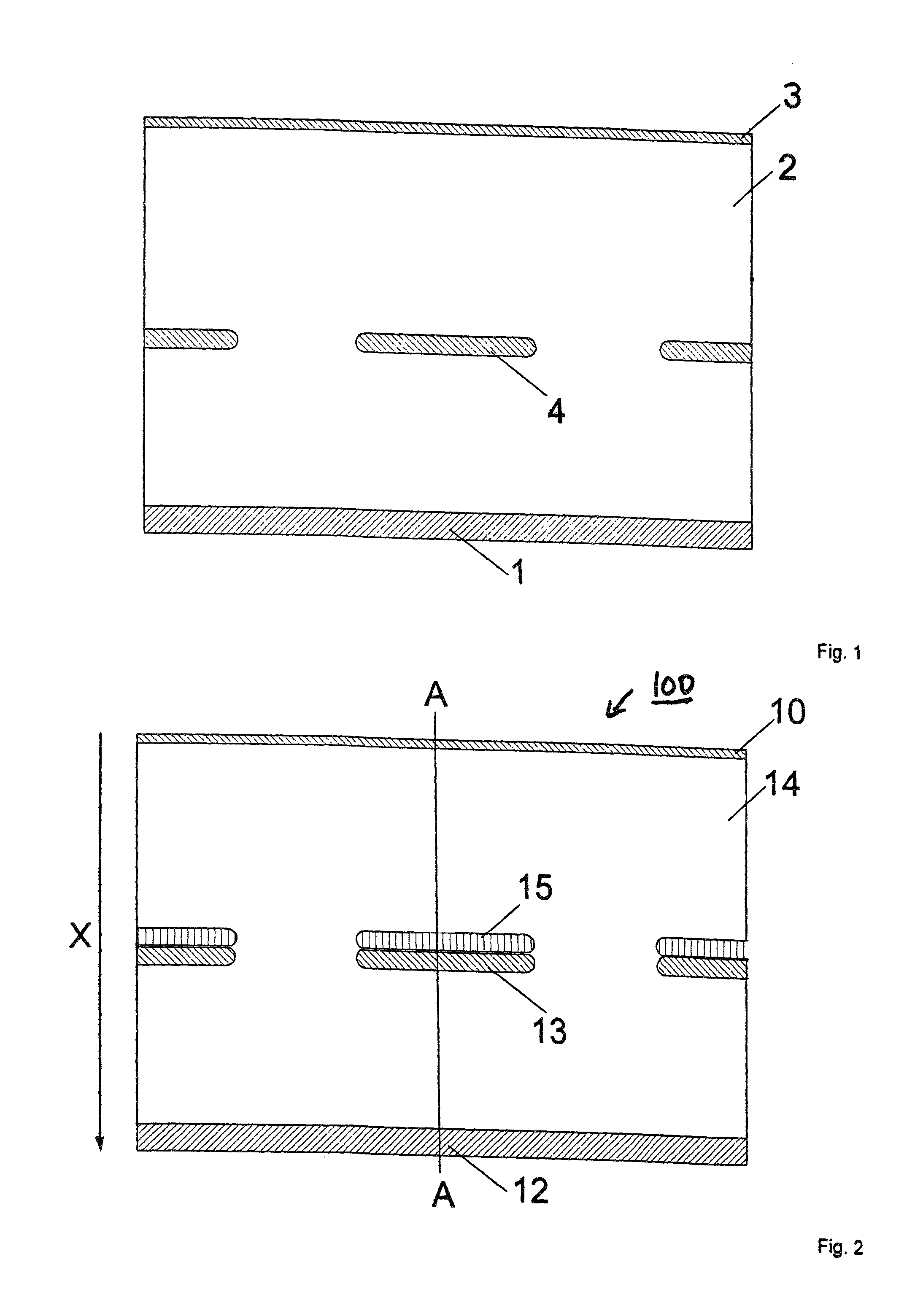
[0048]FIG. 1 shows a schematic view of a known semiconductor detector. A low-resistance p-type semiconductor substrate 2 with an n-conductivity type top diode 3 is arranged on a very low-resistance n-type epitaxial substrate 1. Located in roughly the middle of this arrangement are n-type doping zones 4, which are completely isolated and “float”. Only a small section with three of the doping zones 4 are depicted here. However, real components can exhibit thousands of them, arranged as a matrix or also in hexagonal fields. Disadvantages here include the large operating point voltages for completely depleting the low-resistance layers, and of course the large capacitances of the “floating” st...


PUM


Abstract

A semiconductor structure for a radiation detector, comprising a substrate composed of a semiconductor material of a first conductivity type, a semiconductor substrate, wherein the semiconductor substrate is provided with a semiconductor layer provided on the substrate and having a higher resistance in comparison to the substrate, of the first conductivity type, and electrically doped with a doping concentration, a plurality of doped regions, wherein the plurality of doped regions are provided in the semiconductor substrate and separated from each other, of a second conductivity type that is opposite from the first conductivity type, and electrically doped with a doping concentration that is higher than the doping concentration in the semiconductor substrate, at least one further doping region, and a cover layer is provided.

Description

FIELD OF TECHNOLOGY[0001]The present disclosure relates to technologies in the field of semiconductor radiation detectors, in particular avalanche phototransistors.BACKGROUND[0002]Semiconductor detectors with signal amplification by means of the avalanche effect are often used in radiation receivers for single photon detection.[0003]On the one hand, constructions in use today require a mechanism to keep the field strength above the breakthrough field strength for purposes of single photon detection, the so-called Geiger mode. On the other hand, it should be possible after detection to decrease the breakthrough field so as to be able to detect rapidly following additional photons, so-called “quenching”.[0004]There here exist passive strategies with resistors or semiconductor circuits located outside the semiconductor, and variants actively integrated into the semiconductor, which all have different advantages and disadvantages.[0005]Efforts have been underway for several years to mon...

Claims


Application Information

Patent Timeline
Patent Type & Authority Patents(United States)
IPC IPC(8): H01L31/0352H01L27/144H01L31/107
CPCH01L31/035272H01L27/1446H01L31/107
Inventor PIERSCHEL, MICHAEL
Owner PIERSCHEL MICHAEL
Why Eureka
Try Eureka