
Multilayer structure with high perpendicular anisotropy for device applications

a multi-layer structure and anisotropy technology, applied in the field of multi-layer magnetic stacks, can solve the problems of high temperature, low device integration practicability, and high switching cost, and achieve the effect of low cost and high performan

Active Publication Date: 2014-12-30
HEADWAY TECH INC
View PDF20 Cites 23 Cited by
  • Summary
  • Abstract
  • Description
  • Claims
  • Application Information

AI Technical Summary

Benefits of technology

[0015]One objective of the present invention is to provide a multilayer stack including a seed layer and a (Co / Ni)X or (CoFe / Ni)X laminate formed thereon that has a Hc value substantially greater than 1000 Oe to provide a high performance, low cost alternative to (Co / Pt)Y and (Co / Pd)Y PMA multilayers in magnetic devices such as MRAM, MAMR, and sensors.
[0016]A second objective of the present invention is to provide a (Co / Ni)X or (CoFe / Ni)X multilayer stack with a higher spin polarizing effect and greater Mst than previously achieved in other PMA structures.
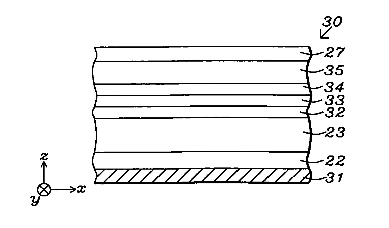
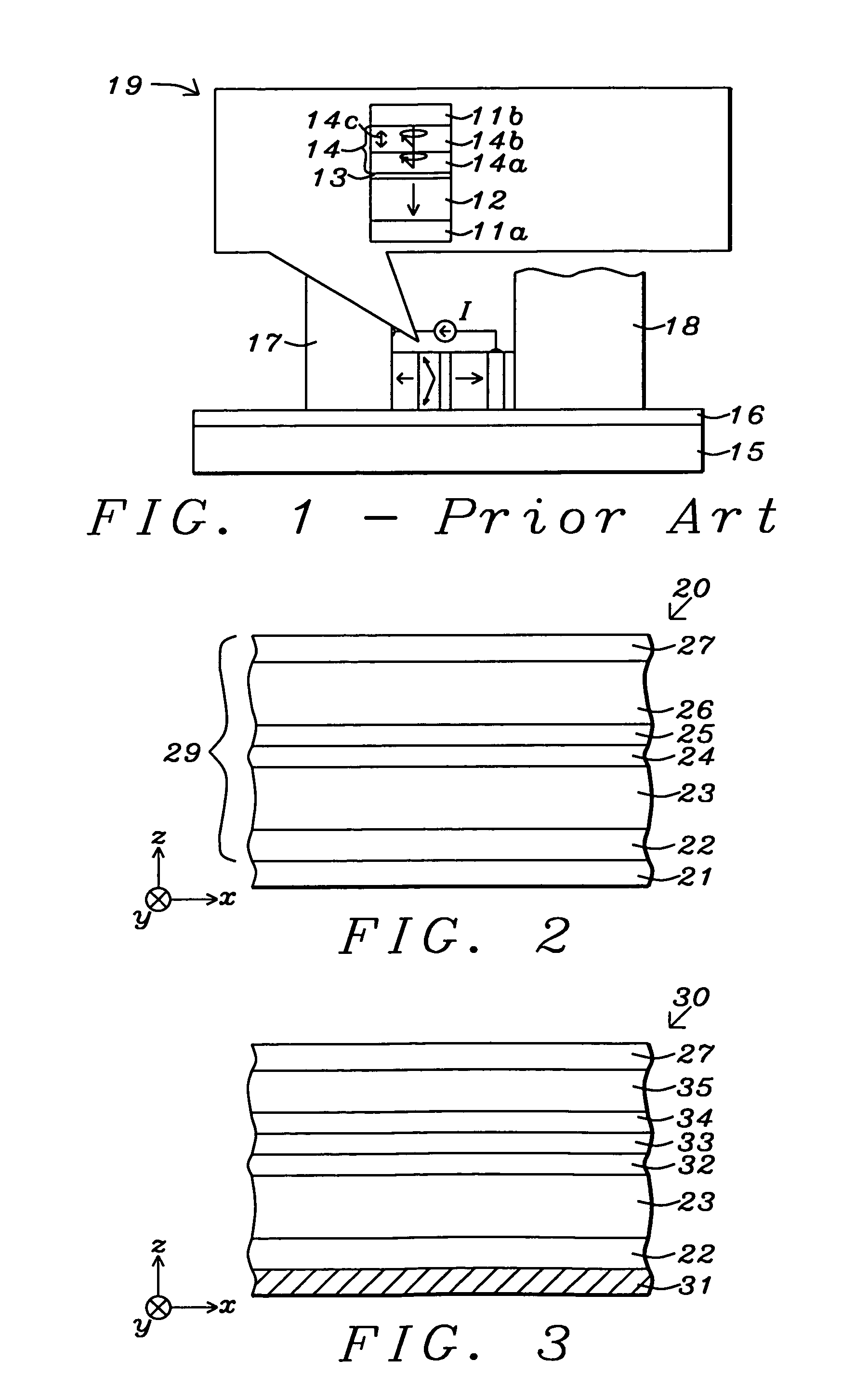
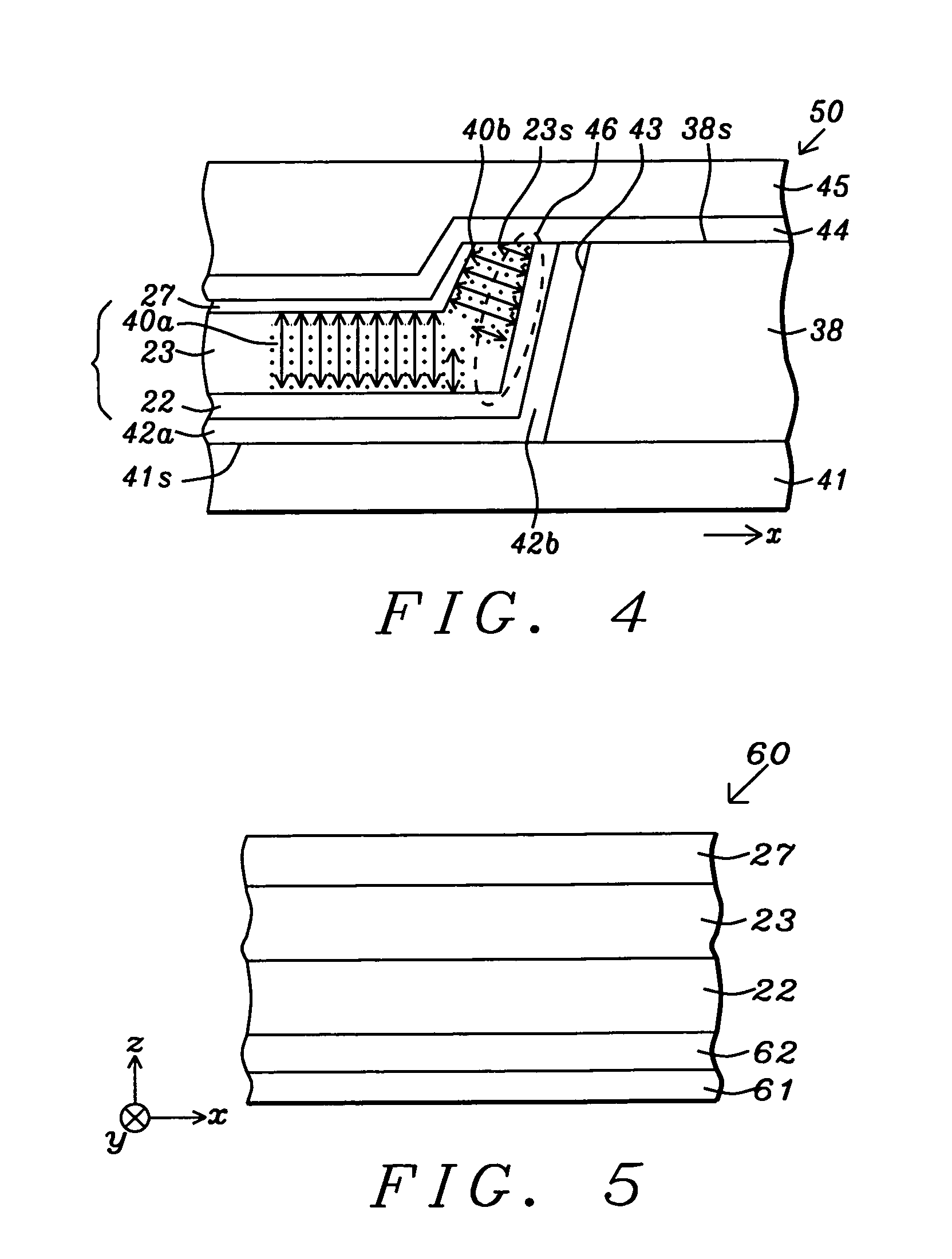
[0017]These objectives are achieved according to the present invention by a stack comprised of a composite seed layer that has a modified top surface to provide enhanced smoothness and an improved interface with an overlying (Co / Ni)X or (CoZFe(100-Z) / Ni)X multilayer where x is from 5 to 50 and z is from 10 to 100 atomic %. Preferably, the composite seed layer is Ta / Ti / Cu where the lower Ta layer contacts a substrate and the Cu layer is the uppermost layer. In one aspect, the seed layer is subjected to a plasma treatment with an inert gas to provide a smoother surface on which the (Co / Ni)X or (CoZFe(100-Z) / Ni)X multilayer stack is deposited. Alternatively, the top surface of the seed layer is subjected to a plasma treatment followed by formation of a thin oxygen surfactant layer. In yet another embodiment, only a natural oxidation of the seed layer top surface is performed to generate a smooth surface on which to deposit the (Co / Ni)X or (CoZFe(100-Z) / Ni)X multilayer stack. Improved interfaces between the Co and Ni or CoFe and Ni layers in the PMA laminate is achieved by employing a low energy, high pressure deposition process to minimize the energy that impinges on the surface of a Co, CoFe, or Ni layer thereby improving the interface with a subsequently deposited layer. Furthermore, in the (Co / Ni)X or (CoZFe(100-Z / Ni)X multilayer stack, one or more of the Co / Ni or CoFe / Ni layers may be treated with a natural oxidation process to form an oxygen surfactant layer (OSL) before a subsequent Co / Ni or CoFe / Ni layer is laid down.

Problems solved by technology

As a result, spin valve structures based on PMA are capable of scaling for higher packing density which is one of the key challenges for future MRAM applications and other spintronic devices.
09). However, in the GMR devices described in the prior art, typical switching current density is above 10 milli-amp / cm2 which is too high for low switching current
MRAM. Furthermore, the MR ratio is around 1% which is too small for the readout signal in
Unfortunately, high temperatures are not so practical for device integration.
CoPt and its alloys such as CoCrPt and CoPt—SiO2 are not desirable as PMA materials in spintronic devices because Pt and Cr are severe spin depolarizing materials and will seriously quench the amplitude of spintronic devices if incorporated in the spinvalve structures.
Similarly, Co / Pd, and Co / Ir will not be good PMA materials for spintronic devices because of the severe spin depolarizing property of Pd and Ir.
Furthermore, Co / Pt, Co / Pd, and Co / Ir configurations typically require a very thick and expensive Pt, Pd, or Ir as a seed layer.
Au is associated with high cost and easy interdiffusion to adjacent layers which makes a Co / Au multilayer for PMA purposes less practical.
However, none of the aforementioned references suggest a high performance, low cost PMA alternative to the commonly used (Co / Pt)Y and (Co / Pd)Y multilayer stacks in the prior art.

Method used


Image

  • Multilayer structure with high perpendicular anisotropy for device applications
  • Multilayer structure with high perpendicular anisotropy for device applications
  • Multilayer structure with high perpendicular anisotropy for device applications

Examples


example 1

[0067]An experiment was performed to demonstrate the improvement in PMA magnitude and Hc when a Ta / Ru / Cu composite seed layer is replaced by a Ta / Ti / Cu composite seed layer as described previously with regard to various embodiments of the present invention. For a reference sample, a partial spin valve stack comprised of a composite Ta10 / Ru20 / Cu20 seed layer, a (Co / Ni)15 laminated layer where each Co layer is 2 Angstroms thick and each Ni layer is 5 Angstroms thick, and a Ru10 / Ta40 / Ru30 cap layer was fabricated in order to obtain PMA values from MH curves using a vibrating sample magnometer (VSM). The thickness of each layer in the composite seed layer and in the composite cap layer is shown by the number following each of the elements. A second sample was prepared by replacing the Ta / Ru / Cu seed layer in the reference with a Ta10 / Ta20 / Cu20 seed layer according to an embodiment of the present invention. Each sample was annealed for 2 hours at 220° C. FIG. 6 shows the perpendicular mag...

example 2

[0068]In a second experiment, partial spin valve stacks with a seed layer / PMA multilayer / capping layer configuration were fabricated to demonstrate the enhanced Hc realized when an ultra high gas pressure is utilized during deposition of a (Co / Ni)X multilayer according to a method of the present invention. As a reference, a stack represented by Ta10 / Ti30 / Cu30 / (Co2 / Ni5)15 / Ru10 / Ta40 / Ru30 was prepared in which the Co and Ni layers were deposited using an Ar flow rate of 100 sccm. A second stack having the same composition was prepared with an ultra high Ar flow rate of 500 sccm. Data in FIG. 7 (graph a) shows Hc=1545 Oe for the perpendicular magnetic field of the reference stack after annealing at 220° C. for 5 hours. In comparison, FIG. 7 (graph b) shows Hc=2130 Oe after the same annealing conditions for the second stack made with ultra high pressure.

example 3

[0069]In a third experiment, the effect of treating a Ta / Ti / Cu seed layer with a PT or NOX process as described earlier is demonstrated. The partial spin valve stack prepared with ultra high pressure in FIG. 7 (b) and FIG. 8 (a) serves as the reference sample and has a composition represented by Ta10 / Ti30 / Cu30 / (Co2 / Ni5)15 / Ru10 / Ta40 / Ru30 in which the seed layer is not treated prior to depositing the (Co / Ni)X multilayer. In a second sample represented by Ta10 / Ti30 / Cu30 / PT / (Co2 / Ni5)15 / Ru10 / Ta40 / Ru30, the composite seed layer is subjected to a plasma treatment involving 20 Watts power, 50 sccm Ar for 50 seconds to form a smoother seed layer surface before the (Co / Ni)15 multilayer and capping layer are deposited. A third sample represented by Ta10 / Ti30 / Cu30 / OSL / (Co2 / Ni5)15 / Ru10 / Ta40 / Ru30 was prepared by performing a NOX process (0.08 sccm oxygen flow rate for 50 seconds) on a Ta10 / Ti30 / Cu30 seed layer before depositing a (Co / Ni)15 multilayer and capping layer. A fourth sample represented...


PUM

PropertyMeasurementUnit
thicknessaaaaaaaaaa
thicknessaaaaaaaaaa
thicknessaaaaaaaaaa

Abstract

Perpendicular magnetic anisotropy and Hc are enhanced in magnetic devices with a Ta / M1 / M2 seed layer where M1 is preferably Ti, and M2 is preferably Cu, and including an overlying (Co / Ni)X multilayer (x is 5 to 50) that is deposited with ultra high Ar pressure of >100 sccm to minimize impinging energy that could damage (Co / Ni)X interfaces. In one embodiment, the seed layer is subjected to one or both of a low power plasma treatment and natural oxidation process to form a more uniform interface with the (Co / Ni)X multilayer. Furthermore, an oxygen surfactant layer may be formed at one or more interfaces between adjoining (Co / Ni)X layers in the multilayer stack. Annealing at temperatures between 180° C. and 400° C. also increases Hc but the upper limit depends on whether the magnetic device is MAMR, MRAM, a hard bias structure, or a perpendicular magnetic medium.

Description

RELATED PATENT APPLICATIONS[0001]This application is related to the following: U.S. Patent Application 2009 / 0257151; Ser. No. 12 / 456,935, filing date Jun. 24, 2009; and Ser. No. 12 / 589,614, filing date Oct. 26, 2009; assigned to the same assignee and herein incorporated by reference in their entirety.FIELD OF THE INVENTION[0002]The invention relates to a multilayer magnetic stack including a seed layer and a (Co / Ni)X or (CoFe / Ni)X laminate with high perpendicular magnetic anisotropy (PMA) and a method for making the same, and in particular, to increasing Hc such that the multilayer magnetic stack is equal to or better in performance compared with more costly (Co / Pt)Y and (Co / Pd)Y systems in a variety of device applications.BACKGROUND OF THE INVENTION[0003]Magnetoresistive Random Access Memory (MRAM), based on the integration of silicon CMOS with MTJ technology, is a major emerging technology that is highly competitive with existing semiconductor memories such as SRAM, DRAM, and Flas...

Claims


Application Information

Patent Timeline
Patent Type & Authority Patents(United States)
IPC IPC(8): G11B5/66G11B5/00G11B5/73G11B5/84G11C11/16G01R33/06G01R33/09G11B5/39
CPCG11B5/732G11B5/66G01R33/098G11C11/16G11B5/84G11B5/7325G11B2005/0024G11B5/3932Y10T428/1114G11C11/161G11C11/1659G11C11/1673G11C11/1675G11B5/7379G11B5/7377H10N50/85H10N50/10H10N50/01
Inventor ZHANG, KUNLIANGLI, MINZHOU, YUCHEN
Owner HEADWAY TECH INC
Learn More