Method of fabricating dielectric layer and shallow trench isolation

a dielectric layer and trench isolation technology, applied in the manufacturing of basic electric elements, electric devices, semiconductor/solid-state devices, etc., can solve the problems of voids and overhangs in the formed sti, and achieve the effect of good gap filling effect, structural completeness and enhanced isolation effect of the dielectric layer

Active Publication Date: 2015-01-06
UNITED MICROELECTRONICS CORP
View PDF28 Cites 4 Cited by
  • Summary
  • Abstract
  • Description
  • Claims
  • Application Information

AI Technical Summary

Benefits of technology

[0008]It is therefore one of the objectives of the present invention to provide a method of fabricating a dielectric layer and a shallow trench isolation (STI) in order to reduce the formation of defects during the dielectric layer process or the STI process.
[0011]Flowable chemical vapor deposition (FCVD) process is performed to form the dielectric layer in the present invention, therefore, the formed dielectric layer can overall cover the substrate, and the recess having high aspect ratio can be totally filled up with the dielectric layer without voids or spaces, i.e. the dielectric layer formed through FCVD process provides good gap filling effect. Additionally, after the planarization process performed on a dielectric layer, the oxygen plasma is further used to treat the surface of the dielectric layer for doping oxygen radicals into a part of the dielectric layer, therefore, the dangling bonds in the dielectric layer may crosslink in order to evaluate the structural density of the dielectric layer, for example, the structure of the upper part of the dielectric layer (penetrated by O radicals) may be denser than the structure of the lower part of the dielectric layer (not penetrated by O radicals). Accordingly, the dielectric layer may not be damaged during the following etching processes and the following cleaning processes, and the structural completeness and the isolation effect of the dielectric layer can be enhanced.

Problems solved by technology

With a trend towards scaling down the size of MOS transistors for achieving high integration rates, when a chemical vapor deposition (CVD) process is used to deposit a dielectric layer to fill the recess, the high aspect ratio of the recess may cause overhang at the top corner of the recess, and voids may be found in the formed STI.

Method used


Image

  • Method of fabricating dielectric layer and shallow trench isolation
  • Method of fabricating dielectric layer and shallow trench isolation
  • Method of fabricating dielectric layer and shallow trench isolation

Examples


Embodiment Construction

[0017]To provide a better understanding of the present invention, preferred exemplary embodiments will be described in detail. The preferred exemplary embodiments of the present invention are illustrated in the accompanying drawings with numbered elements.

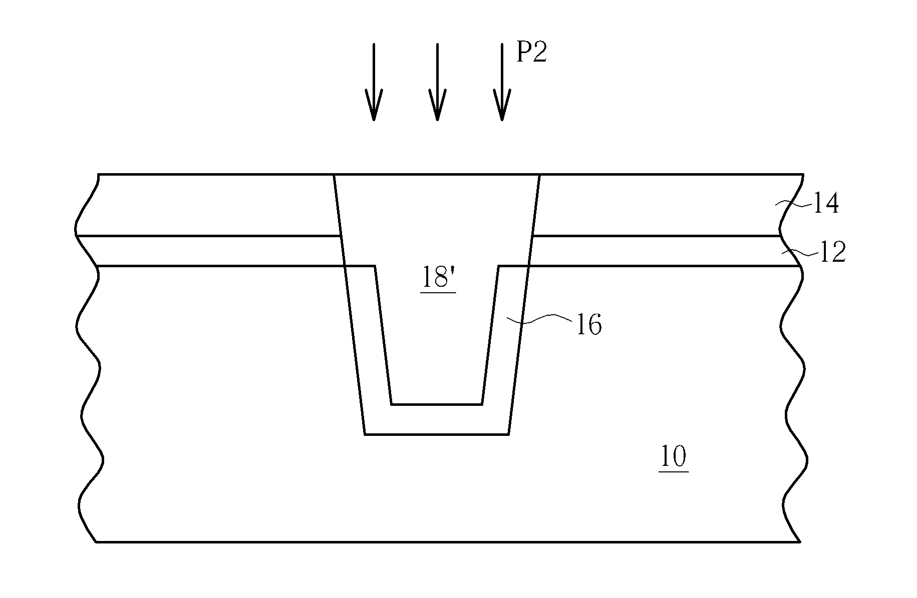
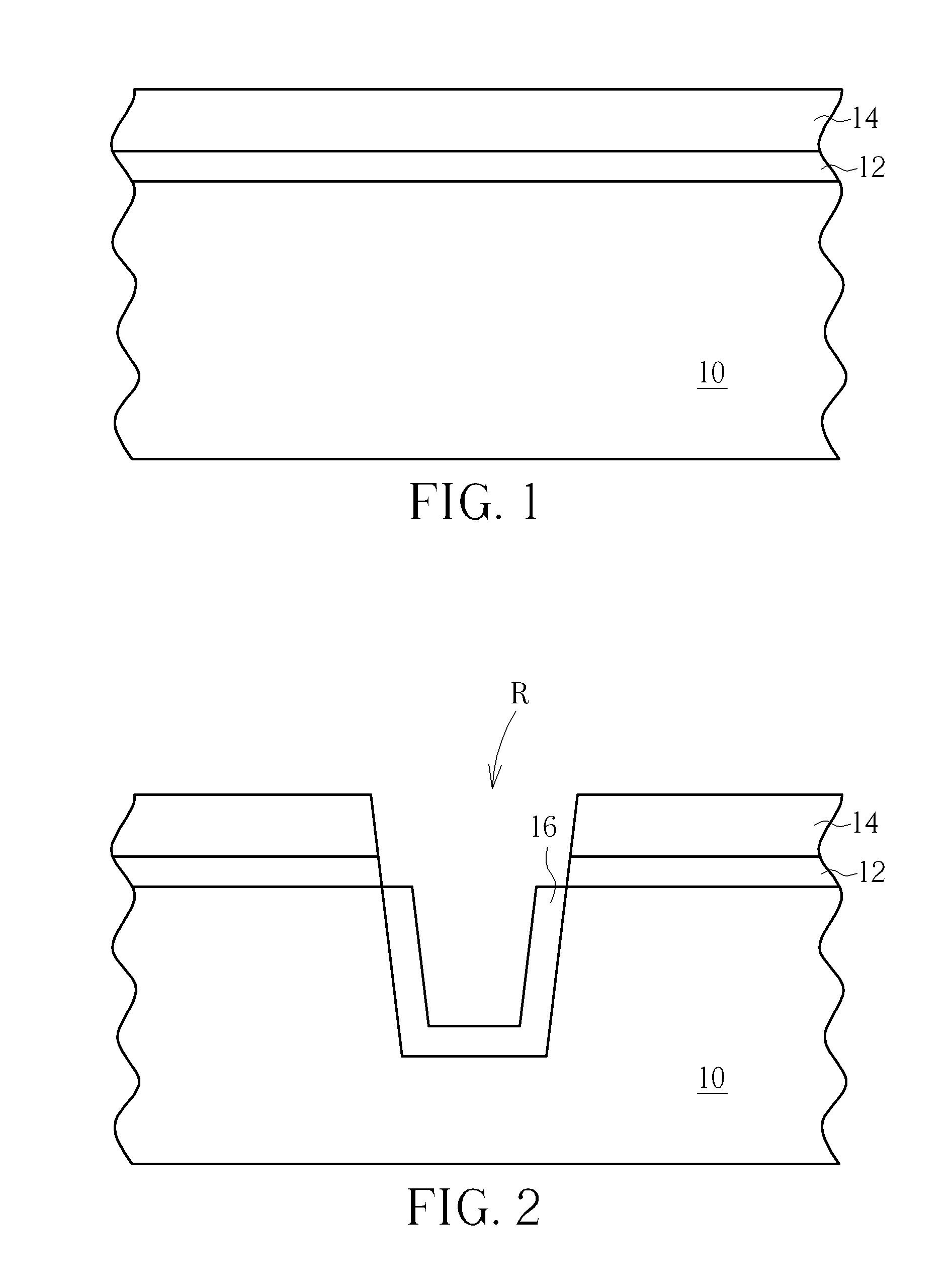
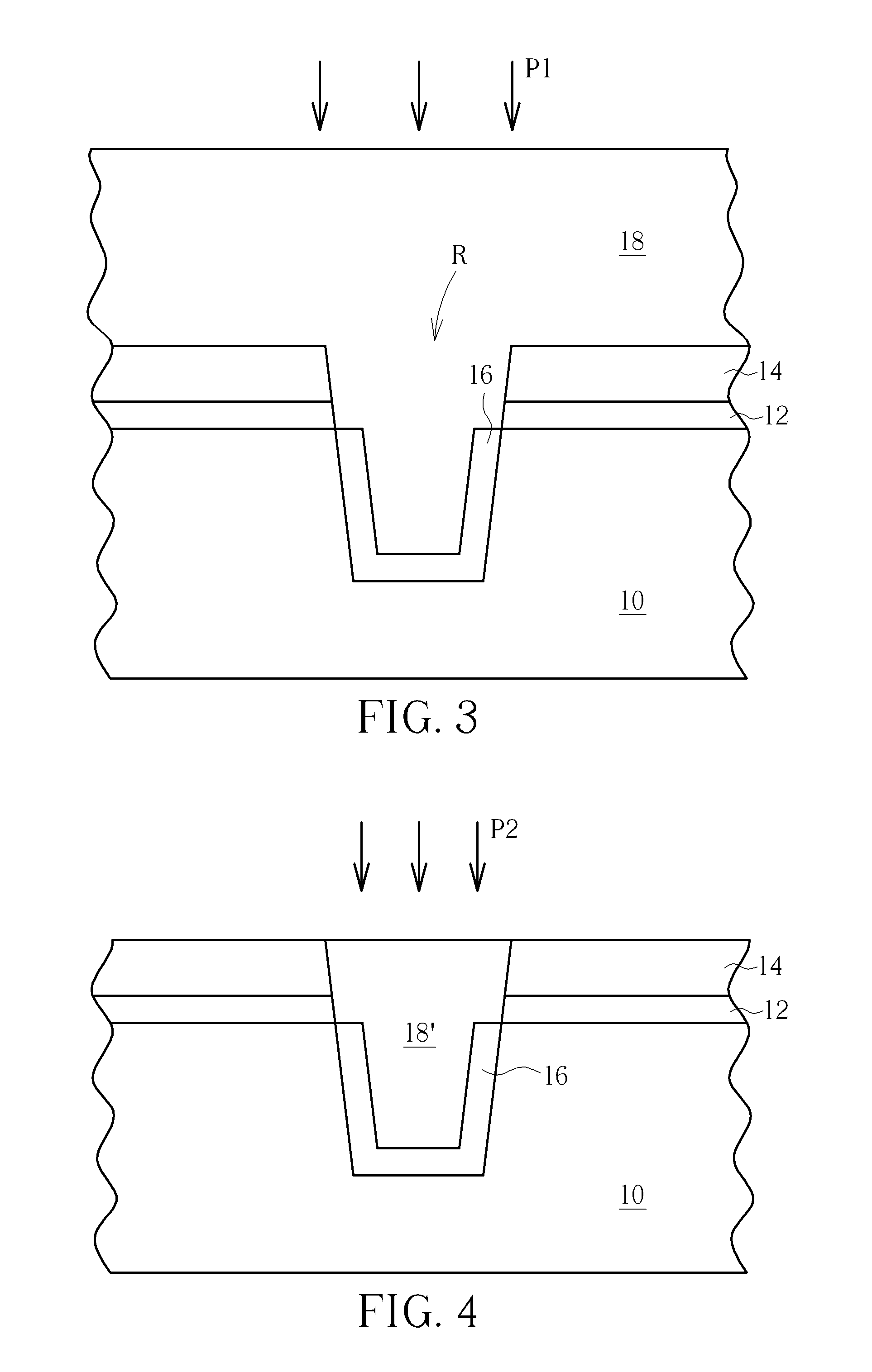
[0018]Please refer to FIG. 1 through FIG. 6, which illustrate a method of fabricating a shallow trench isolation (STI) according to a preferred exemplary embodiment of the present invention. As shown in FIG. 1, a silicon oxide layer 12 which could be formed through thermal oxidation method or chemical vapor deposition process and a silicon nitride layer 14 which could be formed through low pressure chemical vapor deposition (LPCVD) process are sequentially formed on a substrate 10. The substrate 10 may be a semiconductor substrate such as a silicon substrate, a silicon containing substrate, a III-V group-on-silicon (such as GaN-on-silicon) substrate, a graphene-on-silicon substrate or a silicon-on-insulator (SOI) substrate. The sil...


PUM

PropertyMeasurementUnit
temperatureaaaaaaaaaa

Abstract

A method of fabricating a dielectric layer includes the following steps. At first, a dielectric layer is formed on a substrate, and a chemical mechanical polishing (CMP) process is performed on the dielectric layer. Subsequently, a surface treatment process is performed on the dielectric layer after the chemical mechanical polishing process, and the surface treatment process includes introducing an oxygen plasma.

Description

BACKGROUND OF THE INVENTION[0001]1. Field of the Invention[0002]The present invention relates to a method of fabricating a dielectric layer, and more particularly, to a surface treatment process applicable to a dielectric layer of a shallow trench isolation (STI).[0003]2. Description of the Prior Art[0004]In the design of semiconductor devices, each metal-oxide-semiconductor (MOS) transistor component must be well isolated to prevent interference and short-circuiting. In general, localized oxidation isolation (LOCOS) or shallow trench isolation (STI) methods are used to isolate and protect MOS transistors. In the LOCOS process, a field oxide layer occupies a very large area on the semiconductor wafer, and a bird's beak is generated. Therefore, the STI having the advantages of small isolation line width, explicit division of active regions, uniform depth of isolation regions, scalable size and excellent planar structure of isolation regions has become a preferred ideal isolation tech...

Claims


Application Information

Patent Timeline
Patent Type & Authority Patents(United States)
IPC IPC(8): H01L21/76H01L21/02H01L21/3105H01L21/762H01L21/768
CPCH01L21/76224H01L21/3105H01L21/76819H01L21/76826H01L21/76837H01L21/02164H01L21/76229
Inventor CHEN, JEI-MINGTENG, WEN-YICHANG, CHIA-LUNGLIU, CHIH-CHIEN
Owner UNITED MICROELECTRONICS CORP
Why Eureka
Try Eureka