Highly integrated miniature radio frequency module

a radio frequency module, high-frequency technology, applied in the direction of basic electric elements, solid-state devices, electrical apparatus construction details, etc., to achieve the effect of low cos

Active Publication Date: 2015-08-25
VU SYST LLC
View PDF6 Cites 1 Cited by
  • Summary
  • Abstract
  • Description
  • Claims
  • Application Information

AI Technical Summary

Benefits of technology

[0005]This invention is directed to a miniature multi-chip RF module that provides high level of integration, improves circuit performance, and reduces the overall foot print and cost of RF modules. It is therefore an object of the present invention to provide a miniature RF module that overcomes the disadvantages of prior art multi-function modules.
[0006]One aspect of this invention is predicated on the concept of providing a simple, highly integrated miniature module comprising multiple chips and RF circuits arranged in a highly compartmentalized, easily assembled, and lower in cost SMT package. In one embodiment, the miniature module includes a base board formed from a dielectric material and opposing top and bottom metal layers. The top metal layer has radio frequency (RF) circuits and the bottom metal layer has ground and signal pads. Semiconductor chips are mounted to the base board using epoxy or solder and are operative with the RF etched circuits and signal pads for receiving external RF and DC signals and sending RF Signals. A top cover made of machined laminate materials, such as FR-4, with opposing top and bottom metal layers and arrays of metal plated vias extending through the laminate material and connecting the two metal layers, is positioned over the base board to protect the semiconductor chips and RF circuit and provide isolation walls and waveguide channels.

Problems solved by technology

These housings are typically made of expensive coefficient of thermal expansion (CTE) matched material to prevent damage to the semi-conductor chips during temperature cycles.

Method used


Image

  • Highly integrated miniature radio frequency module
  • Highly integrated miniature radio frequency module
  • Highly integrated miniature radio frequency module

Examples


Embodiment Construction

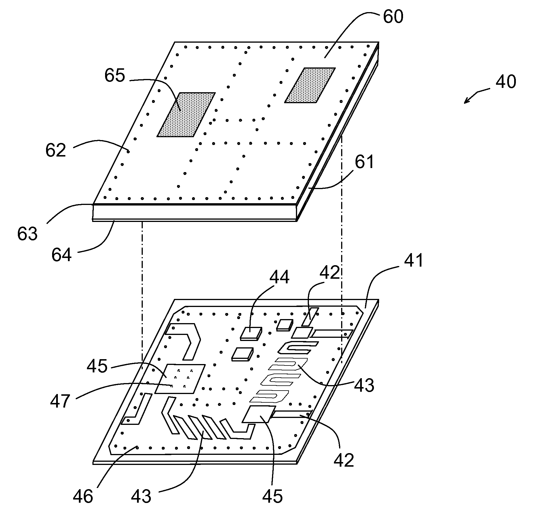
[0020]The present invention will now be described more fully hereinafter with reference to the accompanying drawings, in which preferred embodiments of the invention are shown. This invention may, however, be embodied in many different forms and should not be construed as limited to the embodiments set forth herein. Rather, these embodiments are provided so that this disclosure will be thorough and complete, and will fully convey the scope of the invention to those skilled in the art. Like numbers refer to like elements throughout.

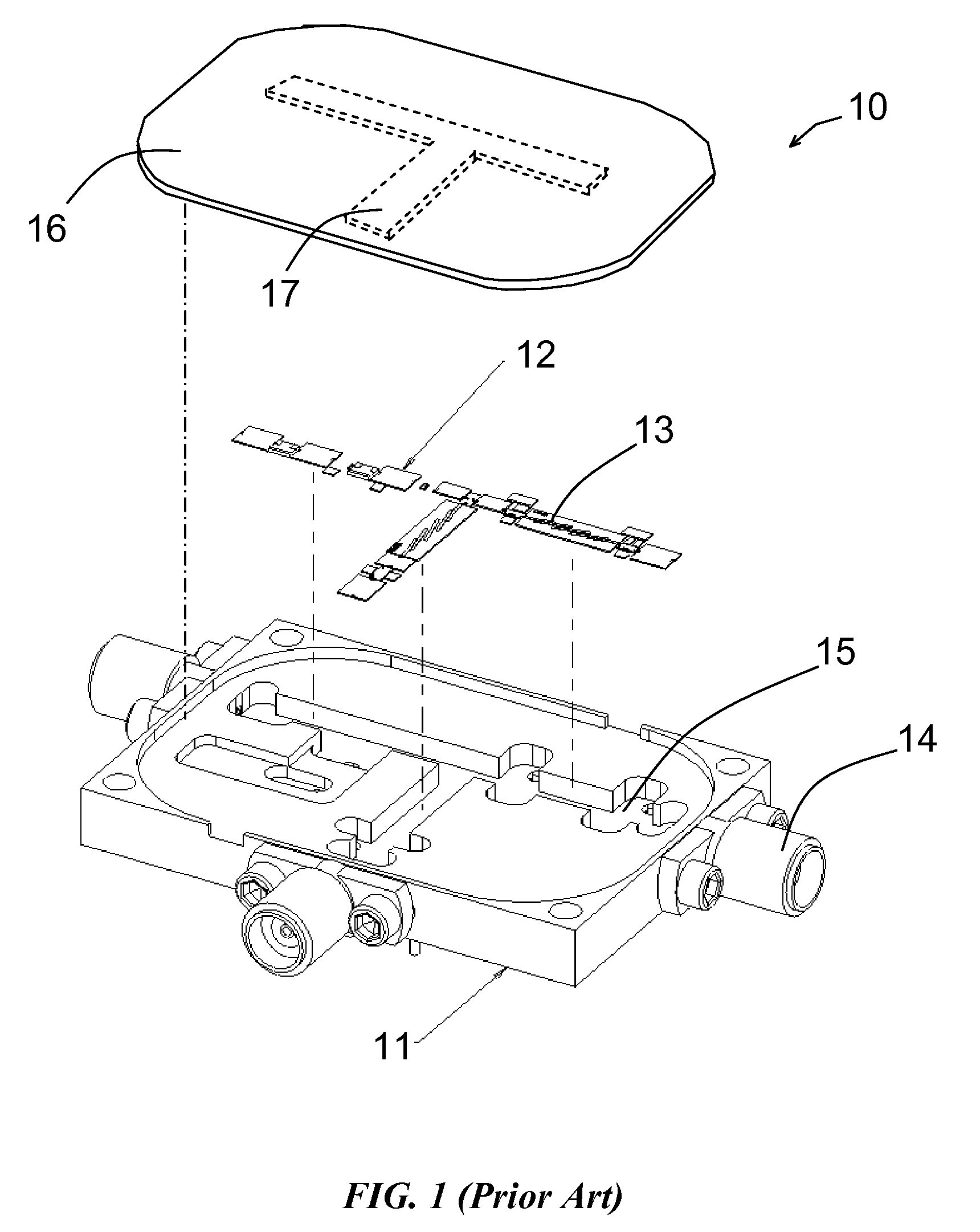
[0021]FIG. 1 illustrates a prior art multi-chip module 10, such as used for high frequency RF transceiver or similar devices, with a housing 11 formed of a CTE matched material, such as copper tungsten (CuW) or aluminum silicon carbide (AlSiC), and used to mount semi-conductor microwave monolithic integrated circuit MMIC die or chips 12 with associated substrates 13 used as interconnects and coupled resonators filters. The housing 11 also includes expensiv...


PUM

PropertyMeasurementUnit
thicknessaaaaaaaaaa
thicknessaaaaaaaaaa
thicknessaaaaaaaaaa

Abstract

A highly integrated miniature RF module includes a dielectric base board with opposing top and bottom metal layers and having interconnects traces, radio frequency (RF) circuits and semiconductor chips at the top metal layer and ground and signal pads at the bottom metal layer. Metalized vias extending through the dielectric material connect the top and bottom layers. A top cover made out of laminate material, such as FR-4, with opposing top and bottom metal layers and having machined compartments and channels, surrounded with arrays of metal plated vias extending through the laminate material, protects the RF circuits and chips and provide the required isolation and wave propagation.

Description

FIELD OF THE INVENTION[0001]This invention relates to Radio Frequency (RF) modules used, for example, in sensors, communication devices or weapon systems, and, more particularly, to a highly integrated, high frequency miniature module that employs a base board with etched traces and RF circuits, a number of semiconductor chips and a channelized cover made of low cost laminate material.BACKGROUND OF THE INVENTION[0002]Multi-chip RF modules, such as transceivers, frequency multipliers, up-converters and down converters, have been designed and built for decades. The most common method used by manufacturers of multi-chip RF modules, is to assemble the chips and RF components in a machined metal housing with expensive waveguide or coaxial interfaces. A Typical high frequency module consists of a number of Microwave Monolithic Integrated Circuit (MMIC) chips, substrates with matched impedance lines and filters, and passive components, all mounted with epoxy or solder to a machined housing...

Claims


Application Information

Patent Timeline
Patent Type & Authority Patents(United States)
IPC IPC(8): H05K7/00H01L25/16H01L23/66H01L23/552
CPCH01L23/66H01L23/552H01L25/16H01L2223/6627H01L2924/0002H01L2924/09701H01L2924/19032H01L2924/19051H01L2924/3011Y10T29/49117H01L2924/00
Inventor AMMAR, DANNY F
Owner VU SYST LLC
Why Eureka
Try Eureka