Superjunction semiconductor device

a semiconductor device and superjunction technology, applied in the direction of semiconductor devices, basic electric elements, electrical appliances, etc., can solve the problems of reducing the reliability of long-term breakdown voltage, difficulty in achieving a structure wherein, and increasing the on-state current, so as to improve the long-term breakdown voltage reliability, improve the charge resistance of the element peripheral portion, and improve the trade-off relationship between breakdown voltage characteristics and voltage drop characteristics.

Active Publication Date: 2015-09-01
FUJI ELECTRIC CO LTD
View PDF13 Cites 3 Cited by
  • Summary
  • Abstract
  • Description
  • Claims
  • Application Information

AI Technical Summary

Benefits of technology

[0010]This invention provides a superjunction semiconductor device in which the trade-off relationship between breakdown voltage characteristics and voltage drop characteristics is considerably improved, it is possible to greatly improve the charge resistance of the element peripheral portion, and it is possible to improve long-term breakdown voltage reliability.
[0012]According to the invention, it is possible to provide a superjunction semiconductor device in which the trade-off relationship between breakdown voltage characteristics and voltage drop characteristics is considerably improved, it is possible to greatly improve the charge resistance of the element peripheral portion, and it is possible to improve long-term breakdown voltage reliability.

Problems solved by technology

However, the higher the breakdown voltage becomes, the higher the resistance and the greater the thickness needed for the drift layer, meaning that it is normally unavoidable that the voltage drop (on-resistance) caused by the on-state current also increases.
That is, in a vertical power semiconductor device, the breakdown voltage characteristics and voltage drop (on-resistance) characteristics are normally conflicting characteristics from the point of view of element structure design, and it is generally considered difficult to achieve a structure wherein both are simultaneously improved.
With the superjunction semiconductor device described in WO2011 / 013379, however, although breakdown voltage charge resistance is ensured at a level of surface charge amount applied to the surface of the element peripheral portion in a range of Qss=±1.0×1012 cm−2, there is a danger of a drop in breakdown voltage in the case of a resin mold seal that has an impurity ion concentration higher than the above level.
That is, a charge resistance at a surface charge amount level of Qss=±1.0×1012 cm−2 is insufficient for the superjunction semiconductor device to be a device of a resin mold seal structure.

Method used


Image

  • Superjunction semiconductor device
  • Superjunction semiconductor device
  • Superjunction semiconductor device

Examples


embodiment 1

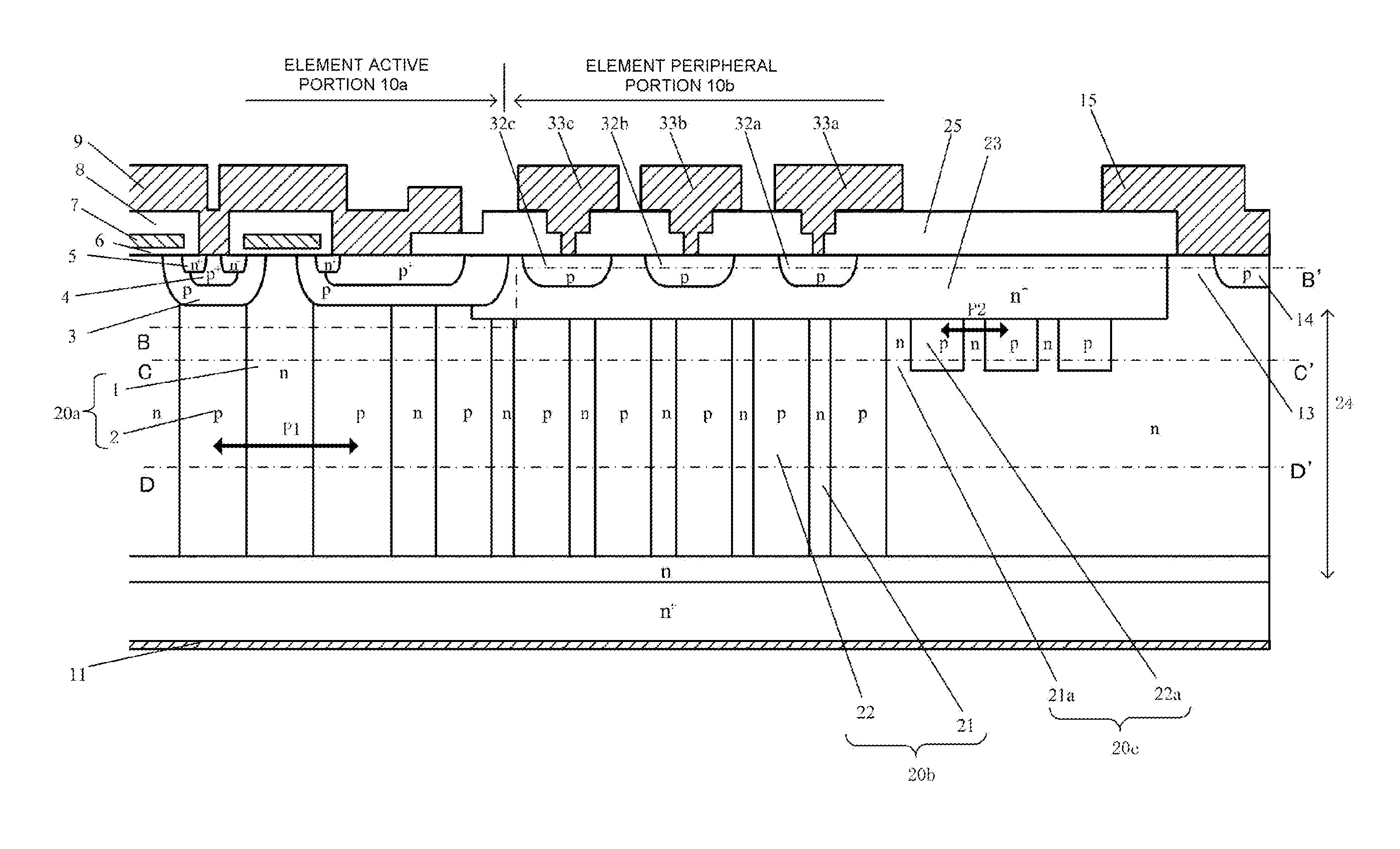
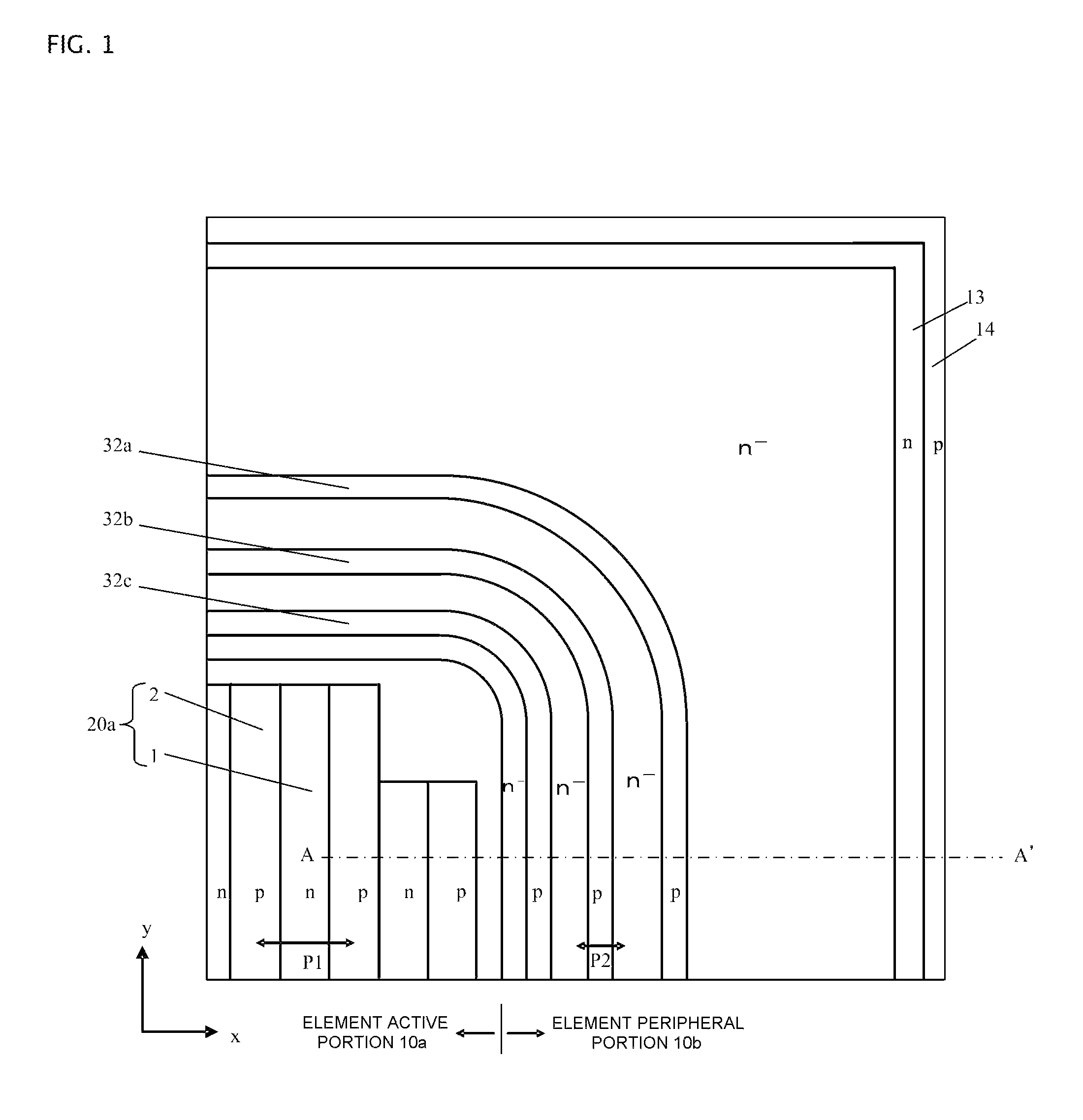
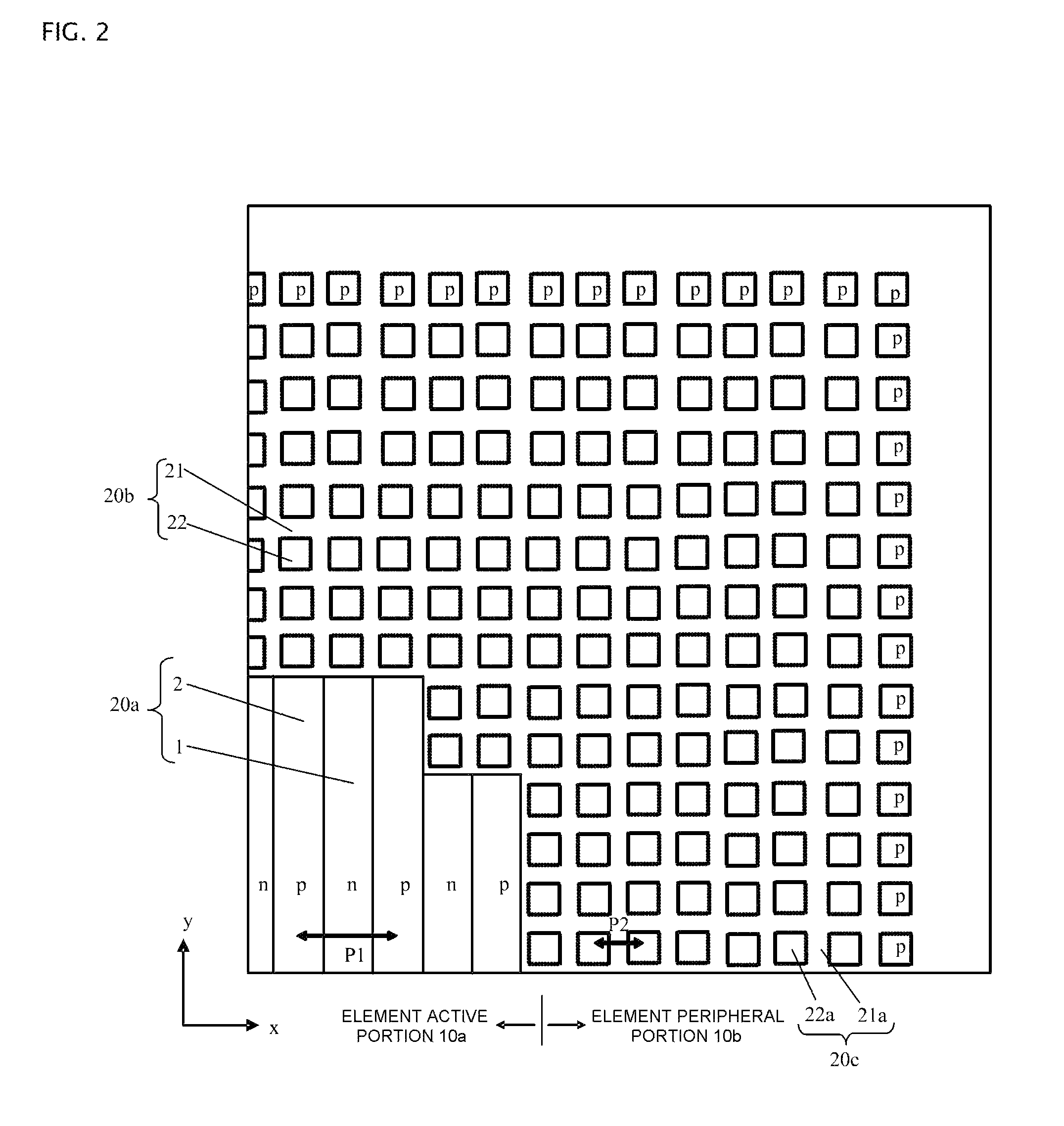
[0031]FIGS. 1, 2, 3, and 4 each show a plan view or sectional view of a vertical superjunction MOSFET (hereafter, element) according to Embodiment 1 of the invention. FIG. 1 shows one portion (a one-fourth element of a quadrilateral chip cut into four equal portions by two perpendicular lines passing through the center of the chip) of a plan view of the element wherein, for ease of understanding, only underlying parallel pn layer 20a is shown in element active portion 10a, while a MOS surface structure disposed in the surface layer of parallel pn layer 20a and source electrode 9 are omitted. FIG. 1 can also be said to be an internal plan view cut along a surface B-B′ (a surface parallel to the main surface) in FIG. 4, to be described hereafter. Element active portion 10a and, as element peripheral portion 10b encircling element active portion 10a, substrate surface p-type guard rings 32a, 32b, and 32c, n− region 23, n-type channel stopper 13 positioned on the outermost side, and p-t...

embodiment 2

[0045]FIG. 11 shows one portion (a one-fourth element) of a transparent plan view of a superjunction MOSFET of Embodiment 2 according to the superjunction semiconductor device of the invention. Although FIG. 11 is the same kind of internal plan view as FIG. 2, it is made a transparent view by a depiction of p-type guard rings 32a, 32b, and 32c being added. In the superjunction MOSFET shown in FIG. 11, the plane pattern of the parallel pn layer of element peripheral portion 10b being of a striped form differs from the superjunction MOSFET of FIG. 2, while other structures are the same as those in FIG. 2. That is, as opposed to Embodiment 1, the plane pattern of parallel pn layers 20b and 20c of element peripheral portion 10b is of a striped form rather than a lattice form, and the depth of p-type partition region 22a is reduced only on the outer peripheral side in element peripheral portion 10b. By reducing the depth of p-type partition region 22a, regardless of the form of parallel ...


PUM


Abstract

A superjunction semiconductor device is disclosed in which the trade-off relationship between breakdown voltage characteristics and voltage drop characteristics is considerably improved, and it is possible to greatly improve the charge resistance of an element peripheral portion and long-term breakdown voltage reliability. It includes parallel pn layers of n-type drift regions and p-type partition regions in superjunction structure. PN layers are depleted when off-state voltage is applied. Repeating pitch of the second parallel pn layer in a ring-like element peripheral portion encircling the element active portion is smaller than repeating pitch of the first parallel pn layer in the element active portion. Element peripheral portion includes low concentration n-type region on the surface of the second parallel pn layer. The depth of p-type partition region of an outer peripheral portion in the element peripheral portion is smaller than the depth of p-type partition region of an inner peripheral portion.

Description

BACKGROUND OF THE INVENTION[0001]A. Field of the Invention[0002]The present invention relates to a superjunction semiconductor device applicable to a MOSFET (insulated gate field effect transistor), IGBT (insulated gate bipolar transistor), bipolar transistor, or the like, with a high breakdown voltage and large current capacity appropriate for a resin mold seal structure.[0003]B. Description of the Related Art[0004]Generally, a vertical power semiconductor device has a structure in which an on-state current flows in a vertical direction between the main surfaces of a semiconductor substrate, and a depletion layer caused by a reverse bias voltage applied to a main junction when turning off extends in the vertical direction between the main surfaces. In order to obtain desired breakdown voltage characteristics in the vertical power semiconductor device, firstly, it is necessary to design a drift layer to a layer resistance and layer thickness commensurate with the desired breakdown v...

Claims


Application Information

Patent Timeline
Patent Type & Authority Patents(United States)
IPC IPC(8): H01L29/66H01L29/06H01L29/78H01L29/08H01L29/10H01L29/40
CPCH01L29/0878H01L29/0619H01L29/0634H01L29/7811H01L29/0638H01L29/0696H01L29/1095H01L29/404
Inventor TAMURA, TAKAHIROONISHI, YASUHIKOKITAMURA, MUTSUMI
Owner FUJI ELECTRIC CO LTD
Why Eureka
Try Eureka