Method for producing a group III nitride semiconductor
a technology of nitride and semiconductor, applied in the direction of semiconductor devices, coatings, chemical vapor deposition coatings, etc., can solve the problems of production cost, and achieve the effect of reducing production cost and good surface flatness and crystallinity
- Summary
- Abstract
- Description
- Claims
- Application Information
AI Technical Summary
Benefits of technology
Problems solved by technology
Method used
Image

Examples
embodiment 1
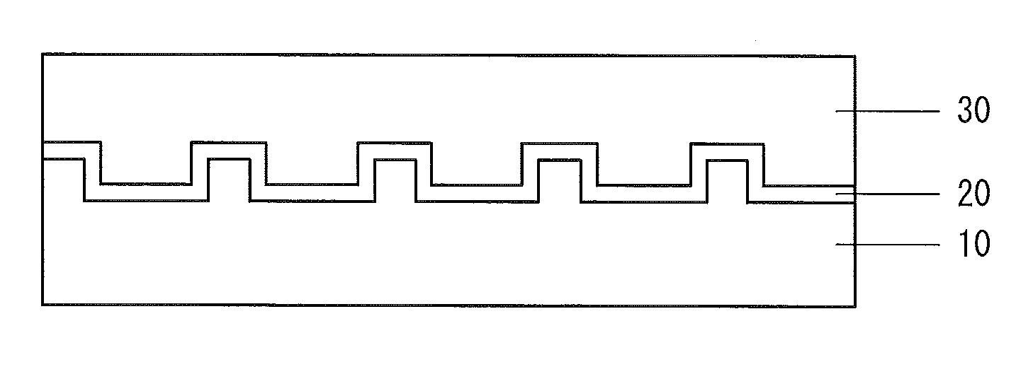
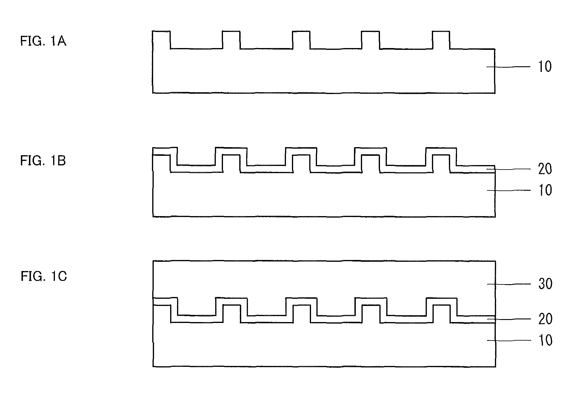
[0031]Firstly, a sapphire substrate 10 having a c-plane main surface was prepared. One surface of the sapphire substrate was patterned by ICP dry etching (FIG. 1A). The pattern includes a dot pattern in which concaves and convexes are periodically arranged or a stripe pattern. In the case of dot pattern, each dot has a planar shape of hexagon, rectangle, triangle, circle, and others, and a three-dimensional shape of pyramid, circular cone, prism, cylinder, truncated pyramid, circular truncated cone, and others which respectively have the above-mentioned planar shape on the top surface of the dot.
[0032]The pattern preferably has a depth (height of dot pattern convex, depth of dot pattern concave, or depth of stripe groove) of 0.1 μm to 10 μm. When the depth is less than 0.1 μm, the light extraction efficiency is not sufficiently improved in the light emitting device according to the present invention. When the depth exceeds 10 μm, the pattern of the Group III nitride semiconductor fo...
embodiment 2
[0040]A method for producing the Group III nitride semiconductor according to Embodiment 2 is the same as the production method according to Embodiment 1 except that thermal treatment is not performed before the formation of the buffer layer 20. That is, while the temperature is kept at a normal temperature without performing thermal treatment after the sapphire substrate 10 was patterned, the AlN buffer layer 20 is formed by magnetron sputtering.
[0041]The method for producing the Group III nitride semiconductor according to Embodiment 2 also allows the formation of Group III nitride semiconductor layer 30 having good surface flatness and crystallinity, similar to the case of the production method according to Embodiment 1. Moreover, since thermal treatment is not performed, the production process can be simplified and the production cost can be reduced. This is because the sapphire substrate 10 is heated by the magnetron sputtering, which substitutes for thermal treatment before th...
embodiment 3
[0043]As shown in FIG. 6A, a sapphire substrate 11 having a c-plane main surface was prepared. One surface of the sapphire substrate was patterned by ICP dry etching to have a periodical concave and convex pattern. The shape, size and concave depth of pattern are the same as those according to Embodiment 1.
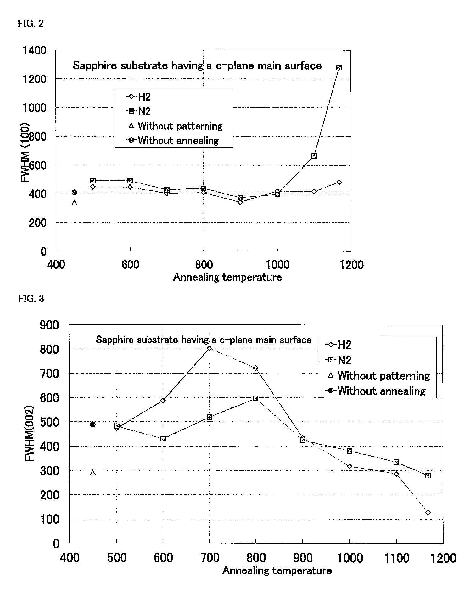
[0044]Subsequently, the patterned sapphire substrate 11 was subjected to thermal treatment in a hydrogen or nitrogen atmosphere at a temperature of more than 800° C. to 1100° C. The pressure was normal. In the thermal treatment, heating was stopped to lower the temperature to a normal temperature immediately after heating to a designated temperature. The thermal treatment may be performed using a magnetron sputtering apparatus used in the next process or other device.
[0045]Next, the patterned sapphire substrate 11 was placed in a chamber of the magnetron sputtering apparatus. With the sapphire substrate 11 heated from 200° C. to less than 700° C., an AlN buffer layer 21 was formed...
PUM
| Property | Measurement | Unit |
|---|---|---|
| temperature | aaaaa | aaaaa |
| temperature | aaaaa | aaaaa |
| temperature | aaaaa | aaaaa |
Abstract
Description
Claims
Application Information
 - R&D
- Intellectual Property
- Life Sciences
- Materials
- Tech Scout
- Unparalleled Data Quality
- Higher Quality Content
- 60% Fewer Hallucinations
Browse by: Latest US Patents, China's latest patents, Technical Efficacy Thesaurus, Application Domain, Technology Topic, Popular Technical Reports.
© 2025 PatSnap. All rights reserved.Legal|Privacy policy|Modern Slavery Act Transparency Statement|Sitemap|About US| Contact US: help@patsnap.com