High performance multigate transistor

a multi-gate transistor, high-performance technology, applied in the direction of semiconductor devices, transistors, electrical devices, etc., can solve the problems of affecting the performance of the device, and reducing the specificity of the device, so as to reduce the parasitic capacitance associated, the device is more sensitive to the transport properties, and the device is more sensitive to the effect of resistan

Active Publication Date: 2015-12-15
QUALCOMM INC
View PDF15 Cites 10 Cited by
  • Summary
  • Abstract
  • Description
  • Claims
  • Application Information

AI Technical Summary

Benefits of technology

[0025]The present invention describes a transistor based on a FET structure, where multiple channels and multiple gate regions are formed in order to achieve a lower specific on-resistance, and a higher control on the transport properties of the device. No dielectric layer is present between gate electrodes and device channels, decreasing the parasitic capacitance associated with the gate terminal. The fabrication of the device does not involve Silicon On Insulator techniques and it is not limited to Silicon semiconductor materials. It can be fabricated as an enhancement or depletion device with much more control on the device threshold voltage, and with superior RF performance.

Problems solved by technology

However the need to further improve on its general performance while reducing its cost is still a necessity that poses a significant challenge.
However, the reduction of Lg alone does not lead to maximum RF performance.
In MESFET structures instead, the main limitation lays in the gate current leakage which is directly correlated to the channel doping and therefore to the RDSon of the device.
Another important limitation of these structures is the difficulty to make them operate as enhancement mode device.
The solution proposed by Ueno et al., even if very efficient in order to obtain an enhancement mode GaN device, still does not offer an improvement of the carrier transport inside the device, such as an increase of the carrier confinement and / or a decrease of short channel effects.
Furthermore, the electron enhancement in the channel portion under the gate is limited (even if an injection of low mobility holes in the channel allows an increase of the electron population).
All these examples, however, require a much more complex and costly process technology involving usually Silicon On Insulator techniques, which are still very expensive nowadays.
A second problem is the alignment of the different gates of the device.
Furthermore, since they are built on buried oxide, they cannot be used for power applications, since their capability to dissipate heat is very poor.
Finally, their solution is limited to Metal-Oxide-Silicon devices, where a dielectric layer is placed between the gate electrode and the channel, increasing the gate capacitance with respect to HEMT and MESFET devices, decreasing the RF performance of the device.
However, also this structure has its limitations, since it does not increase the control on the carrier transport.
Although the cited prior art references describe structures that offer some of the described advantages, no one of them includes all of them, limiting their ability to solve the problem of obtaining transistors with high RF performance, and low on resistance per given semiconductor area in the IC contest.

Method used


Image

  • High performance multigate transistor
  • High performance multigate transistor
  • High performance multigate transistor

Examples


Embodiment Construction
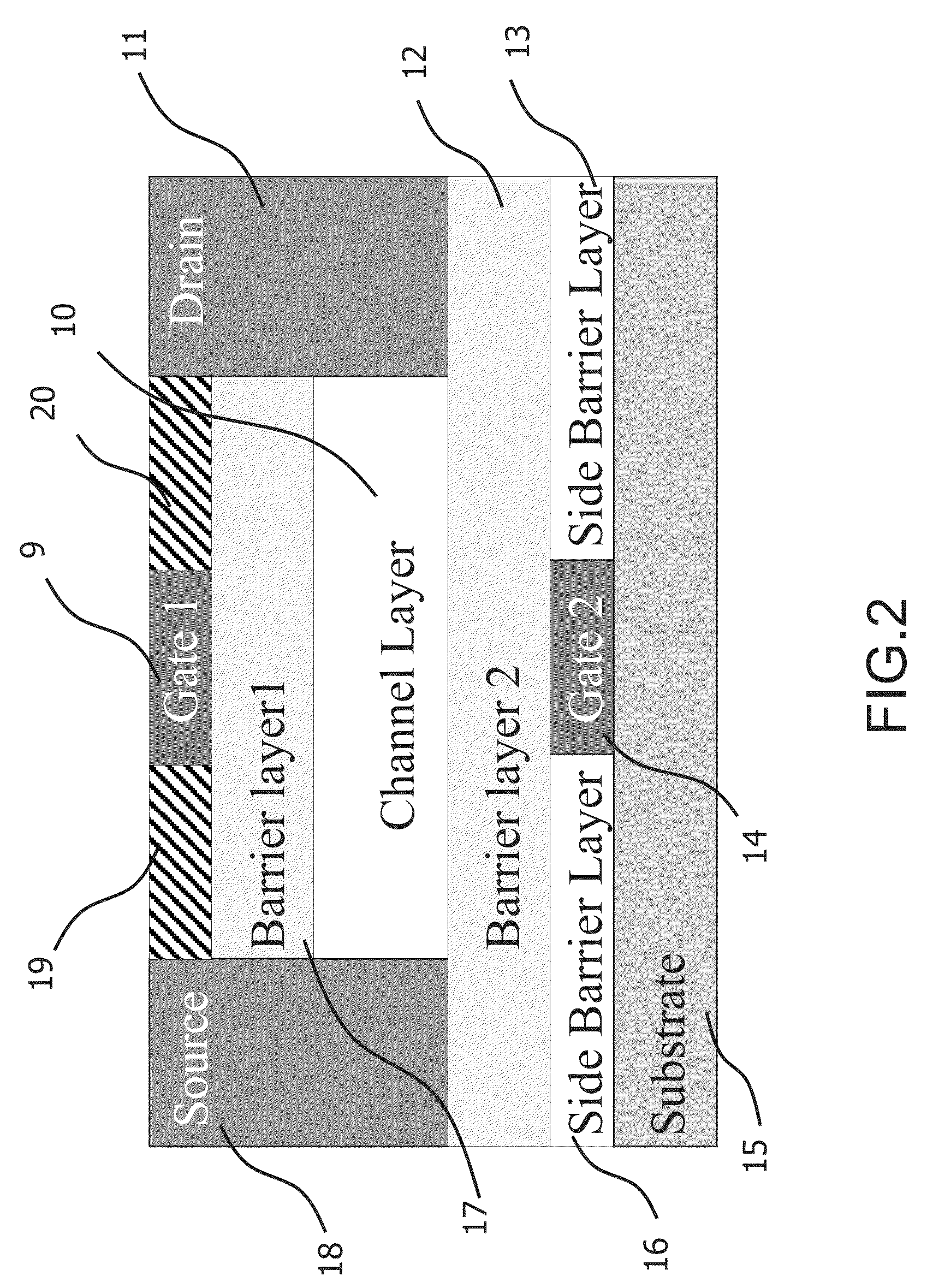
A FIG. 2

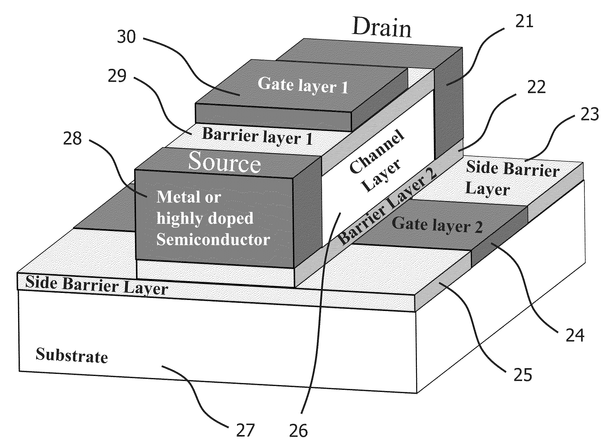
[0076]FIG. 2 is showing a Double Gate HFET (DGHFET) device according to the preferred embodiment of the invention. The metallic or n+-type semiconductor regions 11 and 18 define the drain and the source of the transistor. Regions 17 and 12 corresponds to the two barrier layers of the device, and the channel layer 10 is the region where the electron (or hole)-channels are formed. Region 9, which can be formed using semiconductor materials or metal, corresponds to the first gate of the device, whereas the semiconductor region 14 corresponds to the second gate. As it can be seen, differently from the conventional structure of FIG. 1, where only one electron (or hole)-channel can be identified, in this embodiment a second conductive channel and a second modulation gate have been added to the structure.

[0077]If the desired device is an n-channel HFET, the channel region should have an electron affinity greater with respect to the two barrier layers 17 and 12, in order to confine ...


PUM


Abstract

A novel semiconductor power transistor is presented. The semiconductor structure is simple and is based on a FET structure, where multiple channels and multiple gate regions are formed in order to achieve a lower specific on-resistance, and a higher control on the transport properties of the device. No dielectric layer is present between gate electrodes and device channels, decreasing the parasitic capacitance associated with the gate terminal. The fabrication of the device does not require Silicon On Insulator techniques and it is not limited to Silicon semiconductor materials. It can be fabricated as an enhancement or depletion device with much more control on the threshold voltage of the device, and with superior RF performance.

Description

BACKGROUND OF THE INVENTION[0001]1. Field of the Invention[0002]The present invention is in the field of semiconductor structures. The present invention is further in the field of semiconductor structures of transistor devices. The present invention further relates to the field of integrated devices and circuits. The implementation is not limited to a specific technology, and applies to either the invention as an individual component or to inclusion of the present invention within larger systems which may be combined into larger integrated circuits.[0003]2. Brief Description of Related Art[0004]The semiconductor transistor is the most important component for large integrated circuits. In the last three decades, field effect transistors (FETs) used in current integrated circuit process technologies have undergone a continuous shrinking of the semiconductor area needed for elementary components, and new materials including III-V and II-VI semiconductor compounds have been introduced t...

Claims


Application Information

Patent Timeline
Patent Type & Authority Patents(United States)
IPC IPC(8): H01L29/778H01L29/423H01L29/66H01L29/10H01L29/20
CPCH01L29/7787H01L29/1029H01L29/42316H01L29/66462H01L29/2003
Inventor MARINO, FABIO ALESSIOMENEGOLI, PAOLO
Owner QUALCOMM INC
Why Eureka
Try Eureka