
Eureka
For R&D, Eureka makes reading and utilizing patents & technical documents easy.
Eureka AIR
Designed for self-driven R&D workflows. Generate viable solutions, solve complex R&D challenges, empower your innovation with AI.

Eureka Materials
Designed for material experts only. Revolutionize your material R&D, from search, analyze, to developing new materials.

TechResearch
Generate reliable direction feasibility study reports for your R&D in just a few steps.

TechSeek
Discover and master advanced knowledge NOW. Basics, ideas, possibilities, all at once.

TechMind
As an expert in R&D Theories, TechMind can generates customized viable solutions instantly.

TechRisk
Analyze your overall solution with one click, know your potential R&D risks in advance.

TechMonitor
Get weekly tech updates, stay abreast of the latest tech innovations and key insights.
Microstructure including microstructural waveguide elements and/or IC chips that are mechanically interconnected to each other
- Summary
- Abstract
- Description
- Claims
- Application Information
AI Technical Summary
Benefits of technology
Problems solved by technology
Method used
Image

Examples
Embodiment Construction
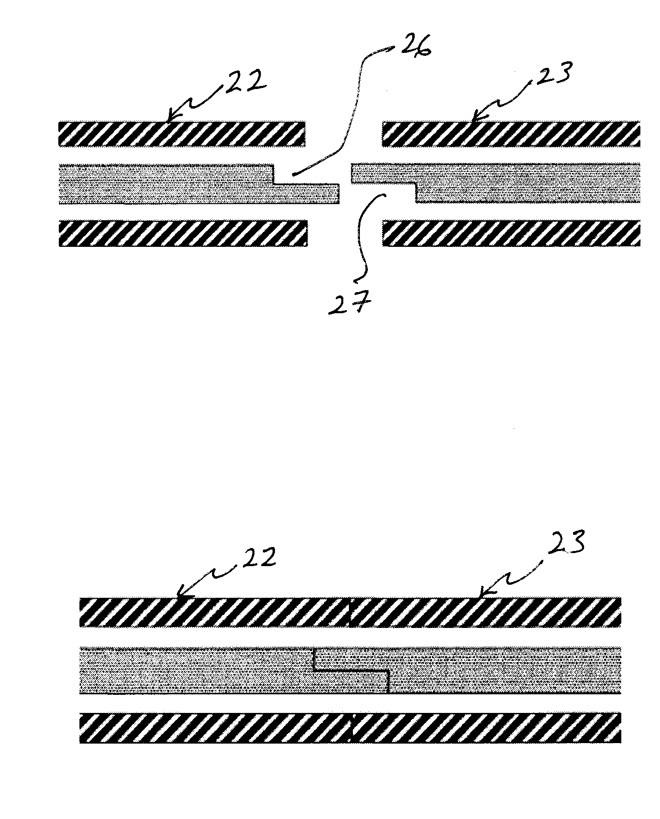
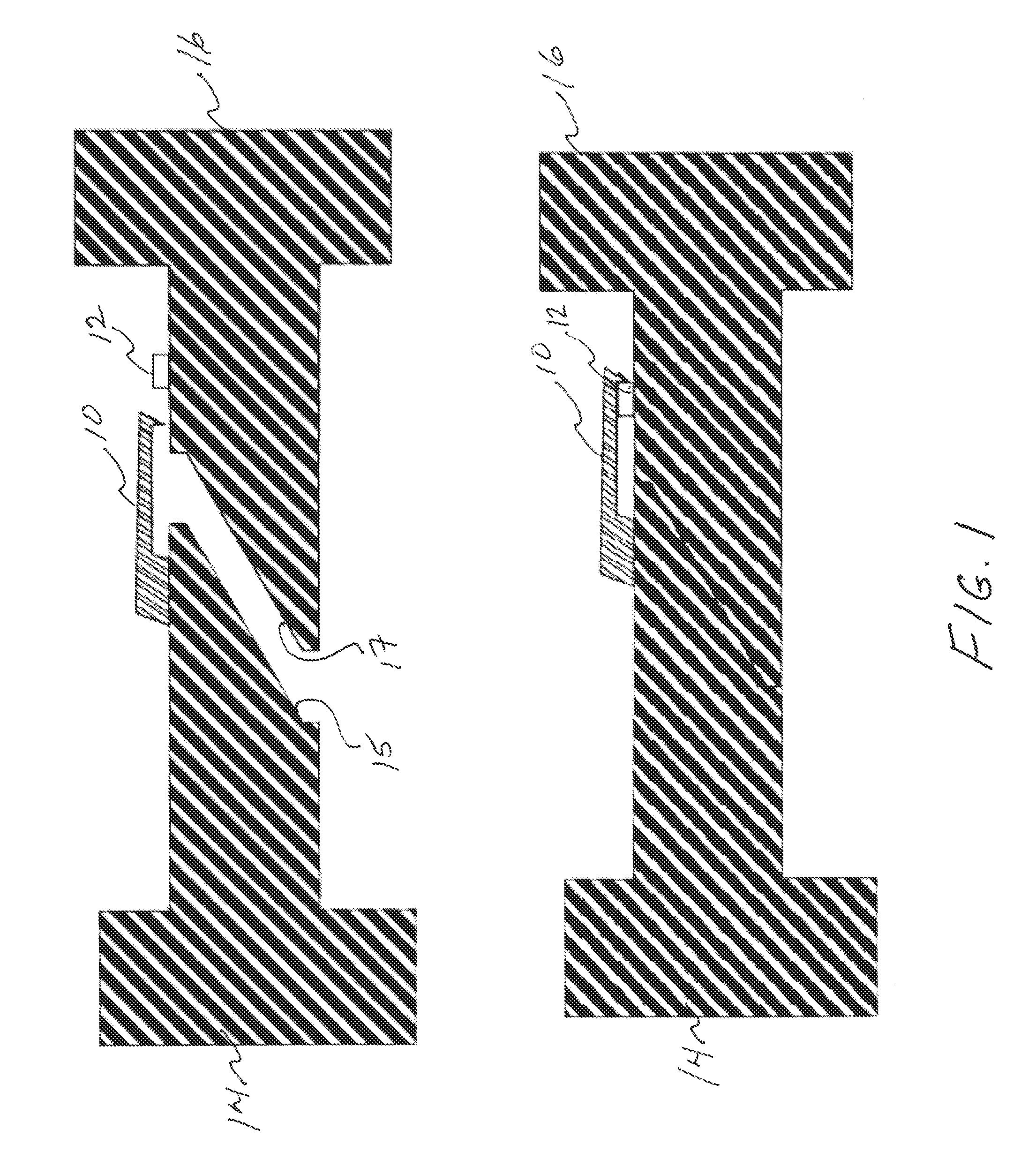
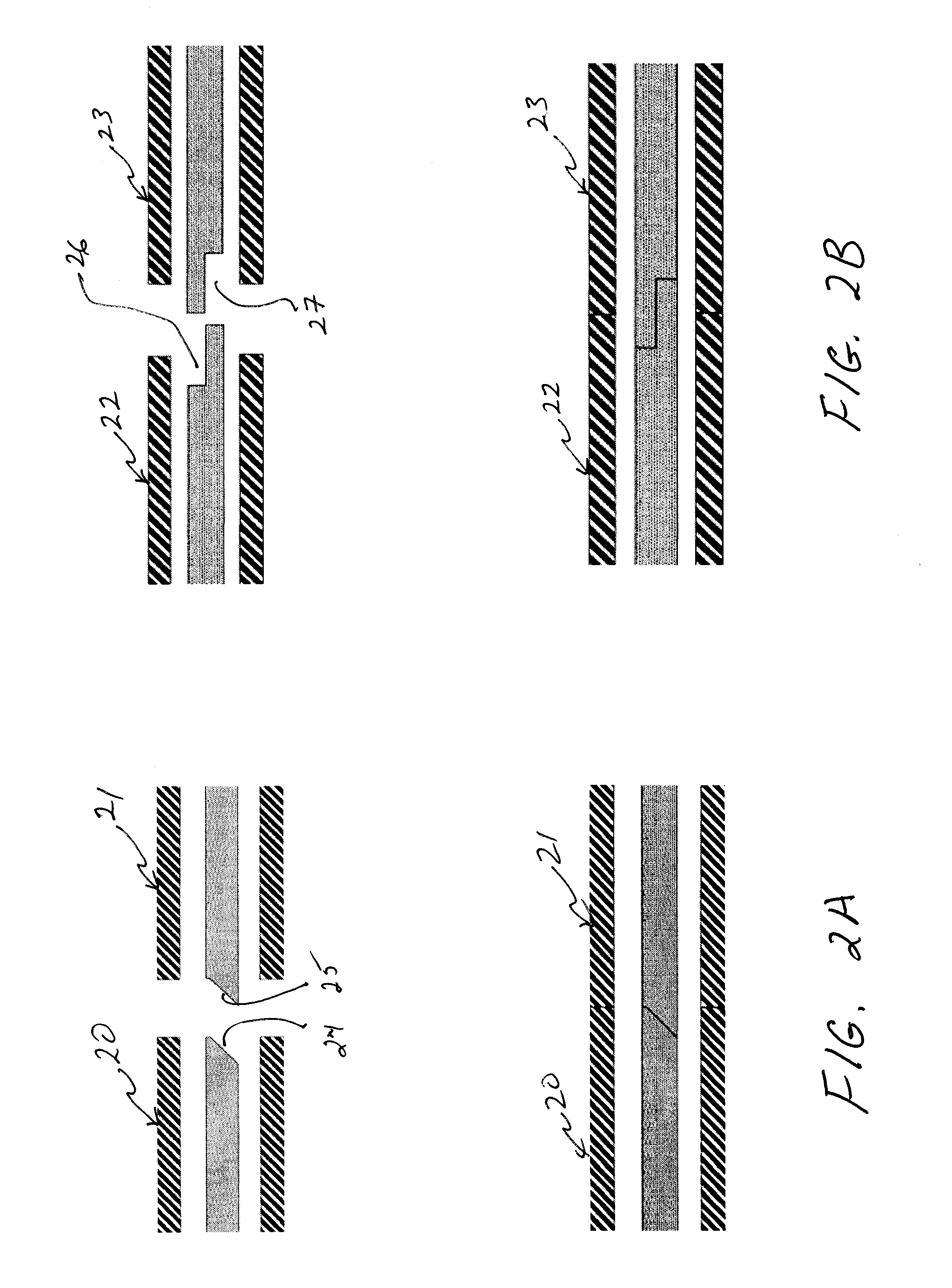
[0049]Referring now to the figures, wherein like elements are numbered alike throughout, the present invention provides several innovations which can help enable systems, such as those described above, to be built with the desired modularity, while precision tolerances and high performance is maintained. For example, in a first inventive aspect the present invention may relate to formation of mechanical structures in monolithically or sequentially formed planar subsystems that provide a spring force or clamping force within microstructured metals and / or dielectrics by a deliberate design and tolerancing of elements disposed therein to create snap-together features that may elastically deform during the interconnection process and still maintain sufficient connection force after being joined. For example first and second subsystems 14, 16 may be operably joined to one another via the action of a latching clip or spring 10 disposed on the first subsystem 14 which latches to a correspo...
PUM
 Abstract
Description
Claims
Application Information
 - R&D Engineer
- R&D Manager
- IP Professional
- Industry Leading Data Capabilities
- Powerful AI technology
- Patent DNA Extraction
Browse by: Latest US Patents, China's latest patents, Technical Efficacy Thesaurus, Application Domain, Technology Topic, Popular Technical Reports.
© 2024 PatSnap. All rights reserved.Legal|Privacy policy|Modern Slavery Act Transparency Statement|Sitemap|About US| Contact US: help@patsnap.com