

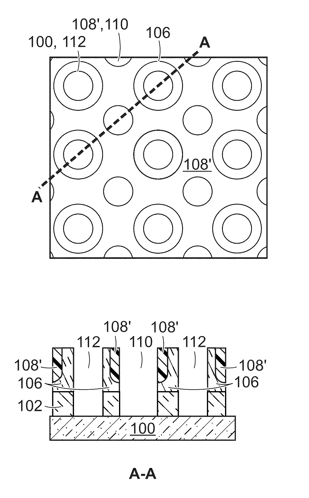
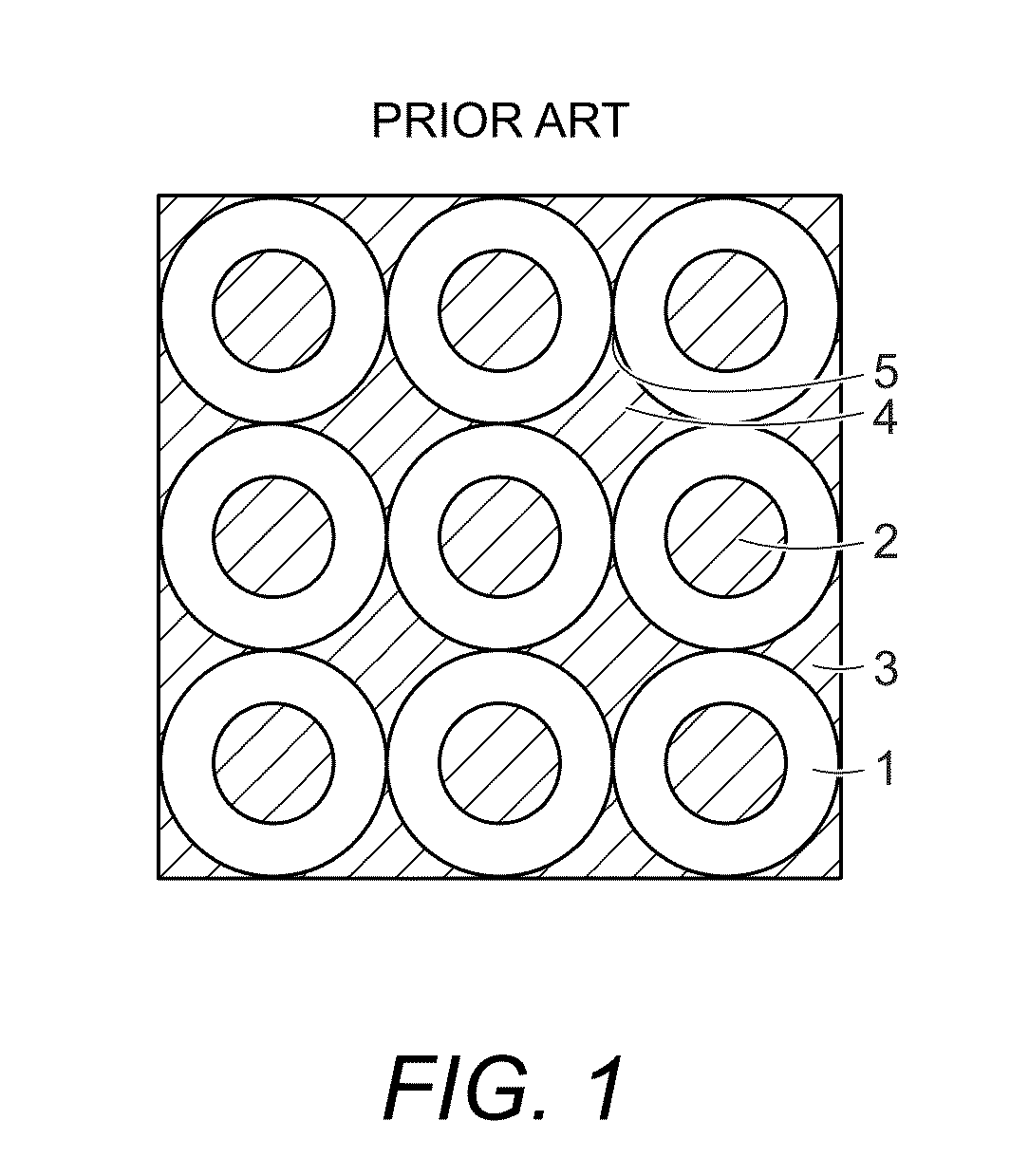
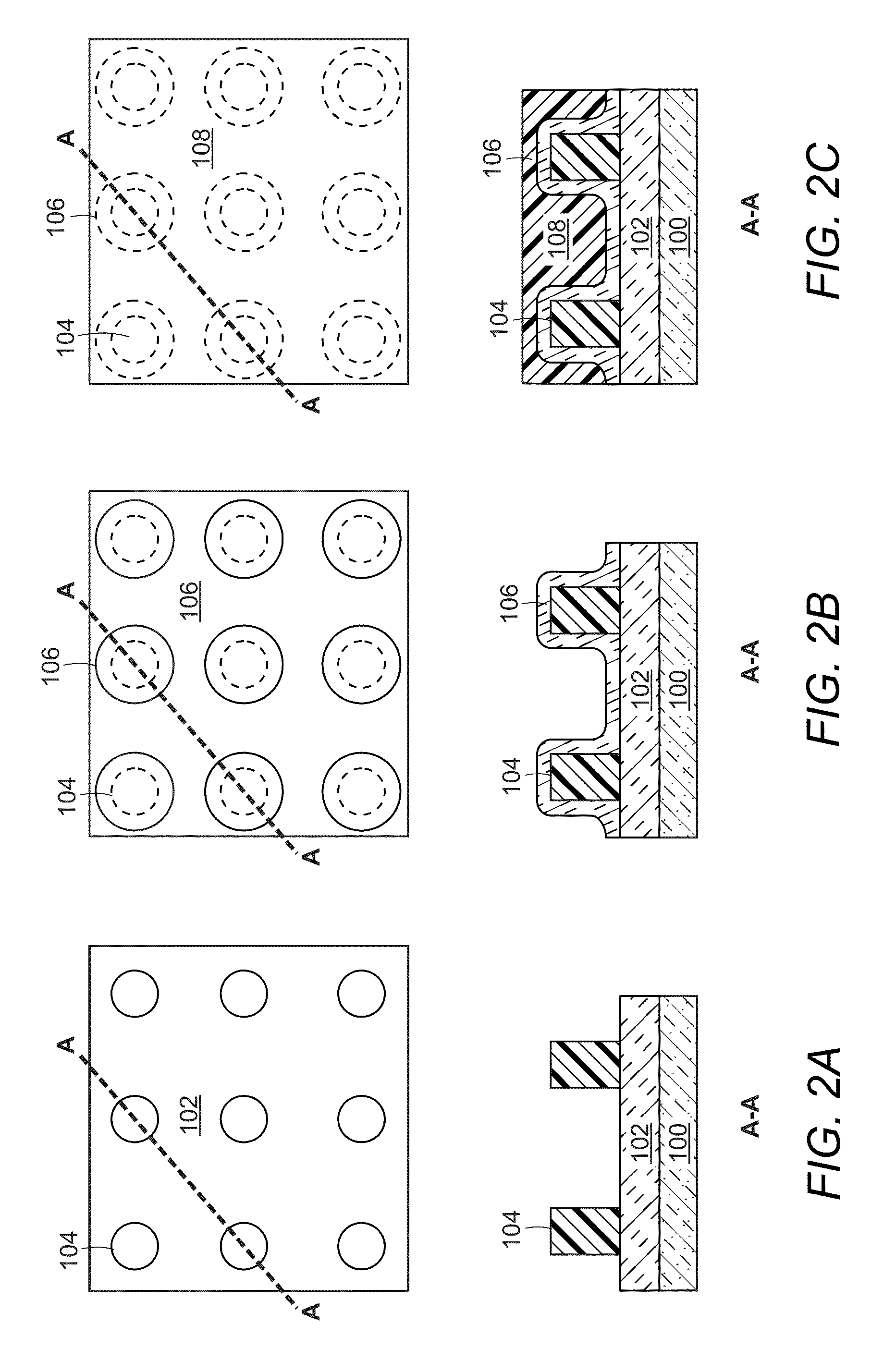
Contact hole formation methods
a technology of contact hole and hole, which is applied in the direction of semiconductor/solid-state device manufacturing, basic electric elements, electric apparatus, etc., can solve the problem of not being able to direct pattern certain features at the resolution needed in next-generation semiconductor devices, the resolution limit of 193 nm immersion scanners, and the delay in widespread adoption of these tools
- Summary
- Abstract
- Description
- Claims
- Application Information
AI Technical Summary
Benefits of technology
Problems solved by technology
Method used
Image

Examples
examples
Pattern Treatment Polymers
Pattern Treatment Polymer-1 (PTP-1)
[0049]0.025 g copper bromide (CuBr), 0.070 g tris[2-(dimethylamino)ethyl]amine and 2 mL anisole were disposed in a sealed sample vial and purged with nitrogen for 15 minutes. In another vial, 0.070 g tin(II) 2-ethylhexanoate was dissolved in 2 mL of anisole and purged with nitrogen. 180.0 g styrene, 0.365 g 2-hydroxyethyl 2-bromo-2-methylpropanoate and 180 mL anisole were added into a 500 mL round bottom flask and purged for 30 minutes with nitrogen. The solutions in the two vials were syringed out and mixed with the contents of and in the 500 mL round bottom flask. The mixture was then reacted by heating with an oil bath for 20 hours at 110° C. After the reaction, the resulting polymer was precipitated from methanol, air-dried overnight, re-dissolved in THF with an ion-exchange resin (Dow Amberlite™ IRC 7481) and re-precipitated from methanol. The final polymer PTP-1 was filtered, air-dried overnight and further dried und...
PUM
 Abstract
Description
Claims
Application Information