
Manufacturing method of organic semiconductor film, organic semiconductor film, thin film transistor, active matrix device, electro-optical device, and electronic device

a manufacturing method and organic semiconductor technology, applied in semiconductor devices, solid-state devices, electrical devices, etc., can solve the problems of remarkably decreasing productivity and yield of organic semiconductor films, low stability of organic semiconductor materials used in liquid phase processes, and effective prevention of variation in properties. , the effect of preventing involuntary variation in properties

Active Publication Date: 2016-11-01
E INK CORPORATION
View PDF8 Cites 0 Cited by
  • Summary
  • Abstract
  • Description
  • Claims
  • Application Information

AI Technical Summary

Benefits of technology

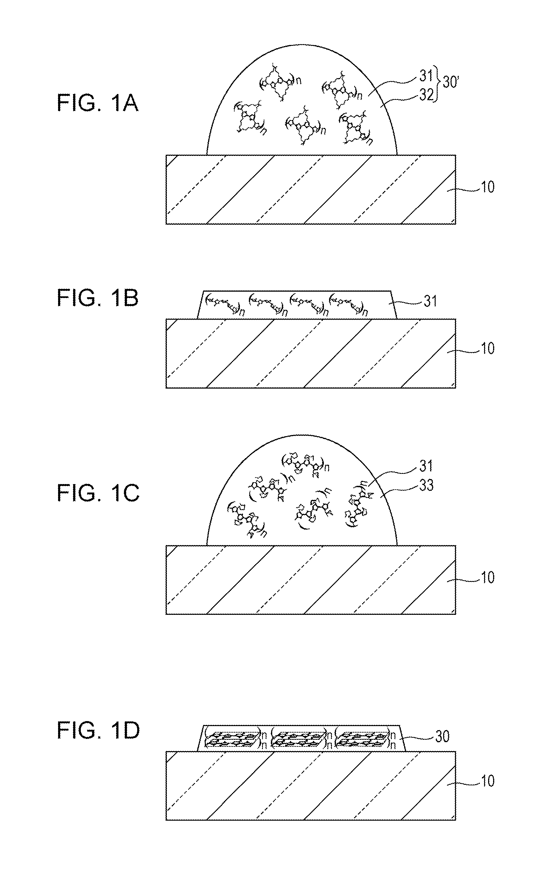
The invention relates to a method for applying a liquid composition (a composition for an organic semiconductor film) onto a base material using different coating methods such as spin coating, casting, and printing. The invention prevents clogging or variation in ejection amount or impact position when using an ink jet method. The liquid composition includes an organic semiconductor material dissolved or dispersed in a solvent, which prevents solid content precipitation or aggregation during storage. The use of a polymer as the organic semiconductor material further prevents variation in properties between films and ensures stability of properties over a long period of time. The invention also provides a specific example of the organic semiconductor material that can be used in the liquid composition.

Problems solved by technology

However, in the related art, stability of a solution of the organic semiconductor material which is used in the liquid phase process is low.
In particular, when the solution is ejected by using an ink jet method, nozzle clogging remarkably occurs, and thus the problem described above becomes remarkable, and productivity and yield of the organic semiconductor film remarkably decrease.

Method used


Image

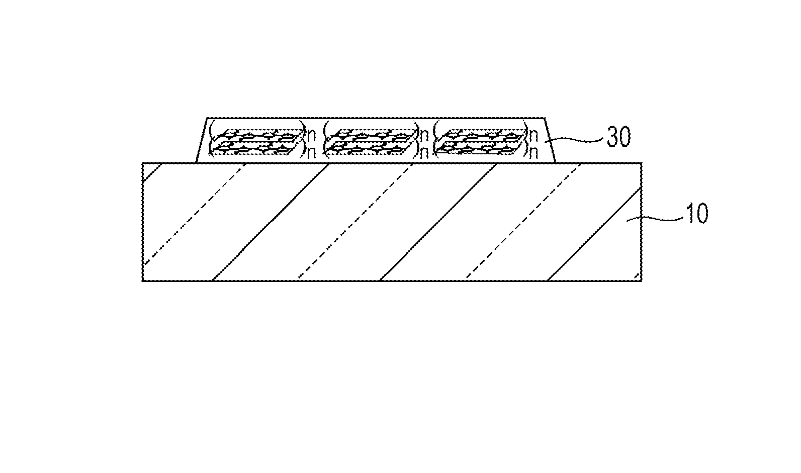
  • Manufacturing method of organic semiconductor film, organic semiconductor film, thin film transistor, active matrix device, electro-optical device, and electronic device
  • Manufacturing method of organic semiconductor film, organic semiconductor film, thin film transistor, active matrix device, electro-optical device, and electronic device
  • Manufacturing method of organic semiconductor film, organic semiconductor film, thin film transistor, active matrix device, electro-optical device, and electronic device

Examples


example 1

1. Source Electrode and Drain Electrode Forming Step

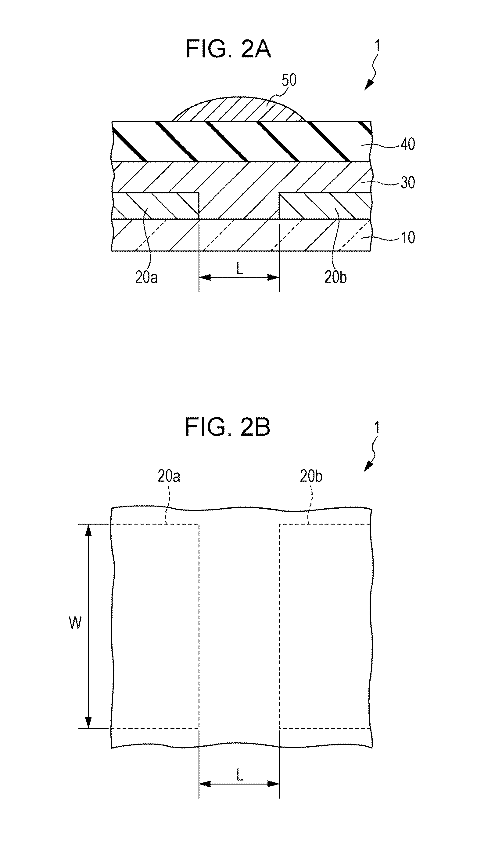
[0200]First, a plastic substrate was prepared, and a degreasing treatment was performed with respect to a surface using ethanol.

[0201]Gold was vapor deposited on the plastic substrate, and thus a source electrode and a drain electrode were formed. After forming the source electrode and the drain electrode, the plastic substrate on which the source electrode and the drain electrode were formed was immersed in isopropyl alcohol, and was subjected to ultrasonic cleaning for 5 minutes. After the cleaning, the substrate was dried at 60° C. for 10 minutes.

2. Liquid Composition Applying Step

[0202]Next, a liquid composition in which poly(3-hexyl thiophene) (P3HT) (a weight-average molecular weight: 30000) as an organic semiconductor material was dispersed in xylene as a first solvent was applied onto the source electrode, the drain electrode, and the substrate by an ink jet method. An applied amount of the liquid composition was determined...

example 2

[0213]A semiconductor device was manufactured by the same method as that in Example 1 except that the configuration of the liquid composition and the second solvent was changed as shown in Table 1.

example 3

[0214]A semiconductor device was manufactured by the same method as that in Example 1 except that the second solvent applying step was performed by exposing a base material having the liquid composition applied thereto into an atmosphere including the second solvent in a vaporized state. In the second solvent applying step, a temperature of the atmosphere was adjusted to 25° C., and a content of the second solvent in the atmosphere was adjusted to 22 g / m3.


PUM

PropertyMeasurementUnit
temperatureaaaaaaaaaa

Abstract

A manufacturing method of an organic semiconductor film according to the invention includes applying a liquid composition in which an organic semiconductor material is dissolved or dispersed in a first solvent onto a base material in a predetermined pattern, applying a second solvent in which solubility of the organic semiconductor material is lower than that in the first solvent onto a region of the base material having the liquid composition applied thereto, and removing the second solvent.

Description

BACKGROUND[0001]1. Technical Field[0002]The present invention relates to a manufacturing method of an organic semiconductor film, an organic semiconductor film, a thin film transistor, an active matrix device, an electro-optical device, and an electronic device.[0003]2. Related Art[0004]Recently, as a device which is able to be substituted for a thin film transistor using an inorganic semiconductor material, a thin film transistor using an organic semiconductor material has received attention (for example, refer to JP-A-2004-6782).[0005]The thin film transistor is able to form an organic semiconductor layer by using a liquid phase process in which high temperature and high vacuum are not necessary.[0006]However, in the related art, stability of a solution of the organic semiconductor material which is used in the liquid phase process is low. For this reason, a solid content in the solution is precipitated or aggregated at the time of preservation, and thus an involuntary variation i...

Claims


Application Information

Patent Timeline
Patent Type & Authority Patents(United States)
IPC IPC(8): H01L51/00H01L51/50H01L51/05H10K99/00
CPCH01L51/0039H01L51/004H01L51/0007H01L51/0036H01L51/0038H01L51/0508H01L51/5004H10K71/15H10K85/141H10K85/113H10K10/464H10K85/115H10K85/114H10K10/46H10K50/11H10K2101/40
Inventor MORIYA, SOICHI
Owner E INK CORPORATION
Learn More