Method for manufacturing insulated circuit board, insulated circuit board, and thermoelectric conversion module

a technology of insulated circuit board and thermoelectric conversion module, which is applied in the direction of printed circuit manufacturing, printed circuit non-printed electric component association, printed circuit aspects, etc., can solve the problems of increasing the manufacturing cost of power modules, reducing the reliability of joining the semiconductor element and the heat sink via the solder material, and forming circuit patterns accurately and efficiently

Active Publication Date: 2020-10-06
MITSUBISHI MATERIALS CORP
View PDF54 Cites 1 Cited by
  • Summary
  • Abstract
  • Description
  • Claims
  • Application Information

AI Technical Summary

Benefits of technology

[0046]According to the present invention, it is possible to provide a method for manufacturing an insulated circuit board capable of accurately and efficiently forming a circuit pattern in a circuit layer including an aluminum layer disposed on one surface of a ceramic substrate and a titanium layer formed on the surface of the aluminum layer on the side opposite to the ceramic substrate, an insulated circuit board, and a thermoelectric conversion module.

Problems solved by technology

Therefore, depending on the solder material, the semiconductor element or the heat sink cannot be directly joined.
However, as described in Patent Document 2, in an insulated circuit board in which the Ni plating film is formed on the surface of the circuit layer and the surface of the metal layer, the surface of the Ni plating film deteriorates due to oxidation and the like in the course of joining the semiconductor element and the heat sink, so that there is a concern that the reliability of joining the semiconductor element and the heat sink joined via the solder material may decrease.
In the case where the plating treatment is performed after the masking treatment as described above, a great effort is needed for the step of forming the Ni plating film on the surface of the circuit layer and the surface of the metal layer, and there is a problem in that the manufacturing cost of the power module greatly increases.
Furthermore, as described in Patent Document 3, in the case where the semiconductor element is joined to the circuit layer using the silver oxide paste and the heat sink is joined to the metal layer using the silver oxide paste, the joining property between the Al and a sintered body of the silver oxide paste is poor; and therefore, there is a need to previously form an Ag underlayer on the surface of the circuit layer and the surface of the metal layer.
Furthermore, in a thermoelectric conversion module, in the case where a circuit layer consists of aluminum or the like, there is a concern that aluminum may diffuse to a thermoelectric element and the characteristics of the thermoelectric element may deteriorate.

Method used


Image

  • Method for manufacturing insulated circuit board, insulated circuit board, and thermoelectric conversion module
  • Method for manufacturing insulated circuit board, insulated circuit board, and thermoelectric conversion module
  • Method for manufacturing insulated circuit board, insulated circuit board, and thermoelectric conversion module

Examples


first embodiment

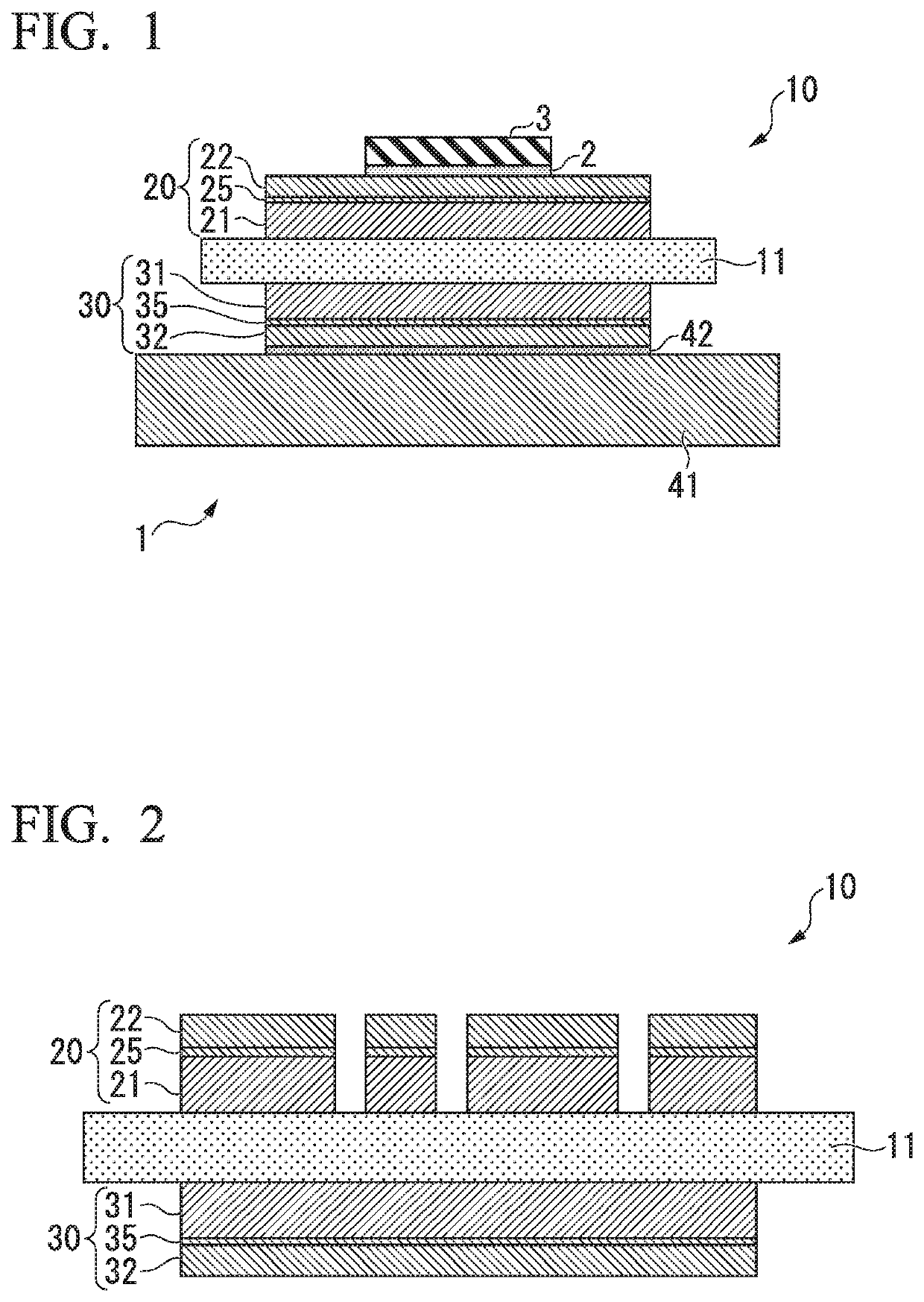
[0061]FIG. 1 shows a power module 1 using an insulated circuit board 10 according to a first embodiment of the present invention.

[0062]The power module 1 includes the insulated circuit board 10, a semiconductor element 3 joined to one surface (upper surface in FIG. 1) of the insulated circuit board 10 via a first solder layer 2, and a heat sink 41 joined to the lower side of the insulated circuit board 10 via a second solder layer 42.

[0063]The semiconductor element 3 includes a semiconductor material such as Si and the like. The first solder layer 2 for joining the insulated circuit board 10 and the semiconductor element 3 together consists of, for example, a Sn—Ag-based, Sn—Cu-based, Sn—In-based, or Sn—Ag—Cu-based solder material (so-called lead-free solder material).

[0064]The heat sink 41 is for dissipating heat on the insulated circuit board 10 side. The heat sink 41 consists of copper or a copper alloy, and in this embodiment, the heat sink 41 consists of oxygen-free copper. The...

second embodiment

[0117]Next, a second embodiment of the present invention will be described. Members having the same configurations as those of the first embodiment are denoted by the same reference numerals, and detailed descriptions thereof will be omitted.

[0118]FIG. 6 shows a power module 101 provided with an insulated circuit board 110 according to the second embodiment of the present invention.

[0119]The power module 101 includes the insulated circuit board 110, the semiconductor element 3 joined to one surface (upper surface in FIG. 6) of the insulated circuit board 110 via a solder layer 2, and a heat sink 141 joined to the lower side of the insulated circuit board 110.

[0120]The heat sink 141 is for dissipating heat on the insulated circuit board 110 side. The heat sink 141 consists of aluminum or an aluminum alloy, and in this embodiment, the heat sink 141 consists of an A6063 alloy. The insulated circuit board 110 and the heat sink 141 are joined together using a brazing filler material.

[012...

third embodiment

[0151]Next, a third embodiment of the present invention will be described. Members having the same configurations as those of the first and second embodiments are denoted by the same reference numerals, and detailed descriptions thereof will be omitted.

[0152]FIG. 10 shows a thermoelectric conversion module 201 provided with insulated circuit boards 210 according to the third embodiment of the present invention.

[0153]The thermoelectric conversion module 201 includes thermoelectric elements 203 and the insulated circuit boards 210 respectively disposed on one end side and the other end side of the thermoelectric elements 203.

[0154]The thermoelectric element 203 is joined to a circuit layer 220 of the insulated circuit board 210 via a joining layer 202. The joining layer 202 is a sintered body of silver paste containing silver particles.

[0155]As shown in FIGS. 10 and 11, the insulated circuit board 210 includes the ceramic substrate 11, and the circuit layer 220 disposed on the one sur...


PUM

PropertyMeasurementUnit
thicknessaaaaaaaaaa
thicknessaaaaaaaaaa
thicknessaaaaaaaaaa

Abstract

The method for manufacturing an insulated circuit board of the present invention includes: a ceramic / aluminum-joining step of joining an aluminum material to a ceramic substrate and thereby, forming an aluminum layer; a titanium material-disposing step of disposing a titanium material on a surface of the aluminum layer or the aluminum material in a circuit pattern shape; a titanium layer-forming step of performing a heat treatment in a state where the titanium material is laminated on the surface of the aluminum layer or the aluminum material and thereby, forming the titanium layer; and an etching treatment step of etching the aluminum layer on which the titanium layer is formed, into the circuit pattern shape.

Description

TECHNICAL FIELD[0001]The invention relates to a method for manufacturing an insulated circuit board including a ceramic substrate and a circuit layer having a circuit pattern disposed on one surface of the ceramic substrate, an insulated circuit board, and a thermoelectric conversion module.[0002]The present application claims priority on Japanese Patent Application No. 2016-124667 filed on Jun. 23, 2016, and Japanese Patent Application No. 2017-121741 filed on Jun. 21, 2017, the contents of which are incorporated herein by reference.BACKGROUND ART[0003]A semiconductor device such as an LED and a power module or a thermoelectric conversion module has a structure in which a semiconductor element or a thermoelectric element is joined onto a circuit layer consisting of a conductive material.[0004]A power semiconductor element for high-power control used for controlling wind power generation, an electric vehicle, a hybrid vehicle, and the like has a large amount of heat generation. Ther...

Claims


Application Information

Patent Timeline
Patent Type & Authority Patents(United States)
IPC IPC(8): H05K3/06H01L23/12H05K1/03H05K1/18H01L23/373H01L23/498H01L35/08H05K3/00H01L23/00
CPCH05K3/0017H01L23/49866H01L23/3735H01L35/08H05K1/0306H05K1/181H05K3/0055H01L23/12H01L2224/29111H01L24/29H01L2224/32225H01L24/83H01L24/32H01L2224/83447H05K2201/10219H01L2924/3512H01L2924/10253H01L2924/01047H01L2924/01029H01L2924/01049H01L2924/00014H05K2201/0341H05K3/062H10N10/817
Inventor TERASAKI, NOBUYUKIOHASHI, TOYO
Owner MITSUBISHI MATERIALS CORP
Why Eureka
Try Eureka