Preparation method of graphene nanoribbon on h-BN

a graphene nanoribbon and nanotube technology, applied in the field of low-dimensional materials and advanced materials, can solve the problems of reducing unable to directly apply to the preparation of electron devices, and limited application thereof, so as to improve the property of graphene, and improve the quality of graphen

Active Publication Date: 2017-02-14
SHANGHAI INST OF MICROSYSTEM & INFORMATION TECH CHINESE ACAD OF SCI
View PDF3 Cites 4 Cited by
  • Summary
  • Abstract
  • Description
  • Claims
  • Application Information

AI Technical Summary

Benefits of technology

[0009]In order to achieve the above object and other related objects, the present invention provides a preparation method of a graphene nanoribbon on h-BN, by which a h-BN groove template with a nano ribbon-shaped groove structure is obtained on h-BN by adopting a metal catalytic etching method, and subsequently a nucleation of a graphene in the nano ribbon-shaped groove structure is achieved to grow the graphene nanoribbon by controlling a CVD growth conditions. The h-BN is known as a “white” graphene, which is insulator, and has a same layered hexagon planar structure with the graphene. The h-BN features an atomically flat surface but without a dangling bond on (0001) plane. The lattice mismatch between the h-BN and the graphene is just about 1.8%, and the doping effect thereof is low, thereby enabling to maintain the intrinsic physical property of the graphene to the greatest extent, and making the h-BN become the most potential insulating substrate of a graphene device. While during the direct growth of a graphene nanoribbon on h-BN, by controlling the metal catalytic etching conditions and CVD reaction conditions, it enables to obtain the graphene nanoribbon with a controllable growth of morphology and structure, so as to achieve the object of improving its electrical properties.
[0031]In the present invention, a CVD method is adopted to directly prepare a morphology controllable graphene nanoribbon on the h-BN, which helps to solve the long-term critical problem that the graphene is difficult to nucleate and grow on an insulating substrate, and to avoid the series of problems introduced by the complicated processes of the transferring of the graphene and the subsequent clipping manufacturing for a nanoribbon and the like. Moreover, the growth of the graphene nanoribbon on the h-BN also has the following remarkable superior effects that, on the one hand, it enables to improve the graphene quality for achieving a high mobility ratio of a charge carrier, on the other hand, by controlling the graphene morphology such as width, marginal structure to realize the regulation of the electron structure of the graphene, it enables to improve the property of the graphene, as well as simplify preparation process of the graphene, reduce production cost, so that the graphene is more widely applicable for the preparation of electron devices.

Problems solved by technology

However, the property of the current graphene is subject to the preparation method and means, and the application thereof is thus limited.
However, the CVD method is catalytic growing a graphene on a transition metal, but fails to be directly applied in the preparation of electron devices, while it is required to transfer the graphene to a dielectric layer to achieve an effective assembled device.
Besides, the transfer process of the graphene adopts a wet chemical method, which not only complicates the technological process, but also inevitably causes a damage and contamination to graphene lattice and thus reduces the quality of the graphene, thereby penalizing the preparation of high-performance electron devices.
Therefore, it has become one of the key problems in graphene photoelectric device on how to avoid the transfer and to overcome the defect of SiO2 / Si substrate.
Moreover, the special crystal structure of the graphene leads to its distinctive zero-energy gap structure, while its metallic characteristic fails to be directly applied in the preparation of electron devices.
Currently, though it is able to prepare graphene of relative few defects and complete structure, but the band gap of the obtained graphene is almost zero or quite small, which can hardly meet the requirements for semiconductor functional devices.
Nevertheless, the application of the graphene is limited in the electronics field due to its zero-band gap structure.
However, in those methods for regulating the electron structure of the graphene, it is required to prepare a graphene of complete structure, followed by performing modified regulation, which is subject to a restriction of process technology, and a non-control of doping concentration, etc.
Also, from an electron device manufacture and a commercialization perspective, the process is tedious and is high in cost.
From the above, the development of the graphene faces the following challenges: its application in the field of nanoelectronic device and integrated circuits is limited by the electron structure of the zero-band gap of the graphene; the electrical property of the graphene material is far inferior to its intrinsic electrical property because of the introduction of defects and electric charge impurities in the existing preparation and transfer technology of graphene.

Method used


Image

  • Preparation method of graphene nanoribbon on h-BN
  • Preparation method of graphene nanoribbon on h-BN
  • Preparation method of graphene nanoribbon on h-BN

Examples


Embodiment Construction

[0044]The embodiment modes of the present invention are described hereunder through specific examples, and persons skilled in the art may easily understand other advantages and efficacies of the present invention from the contents disclosed in the present description. The present invention may be further implemented or applied through other different specific embodiment modes, and various modifications or amendments may also be made to each of the details in the present description based on different perspectives and applications without departing from the spirit of the present invention.

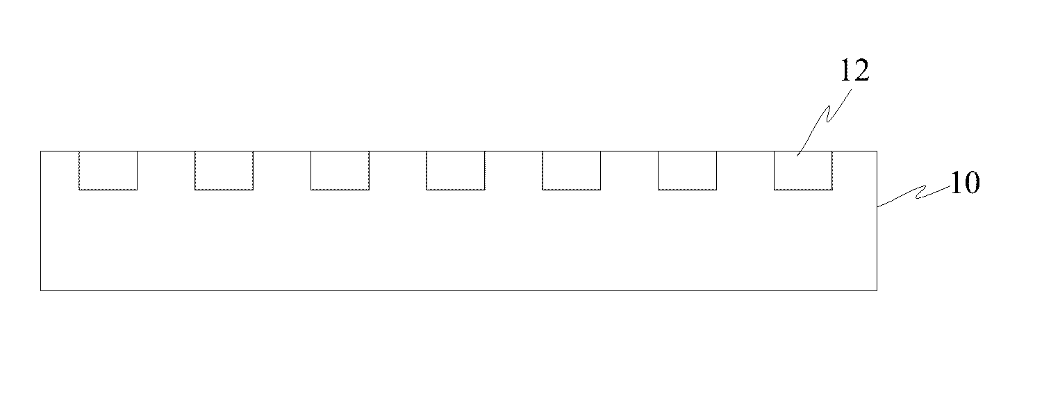
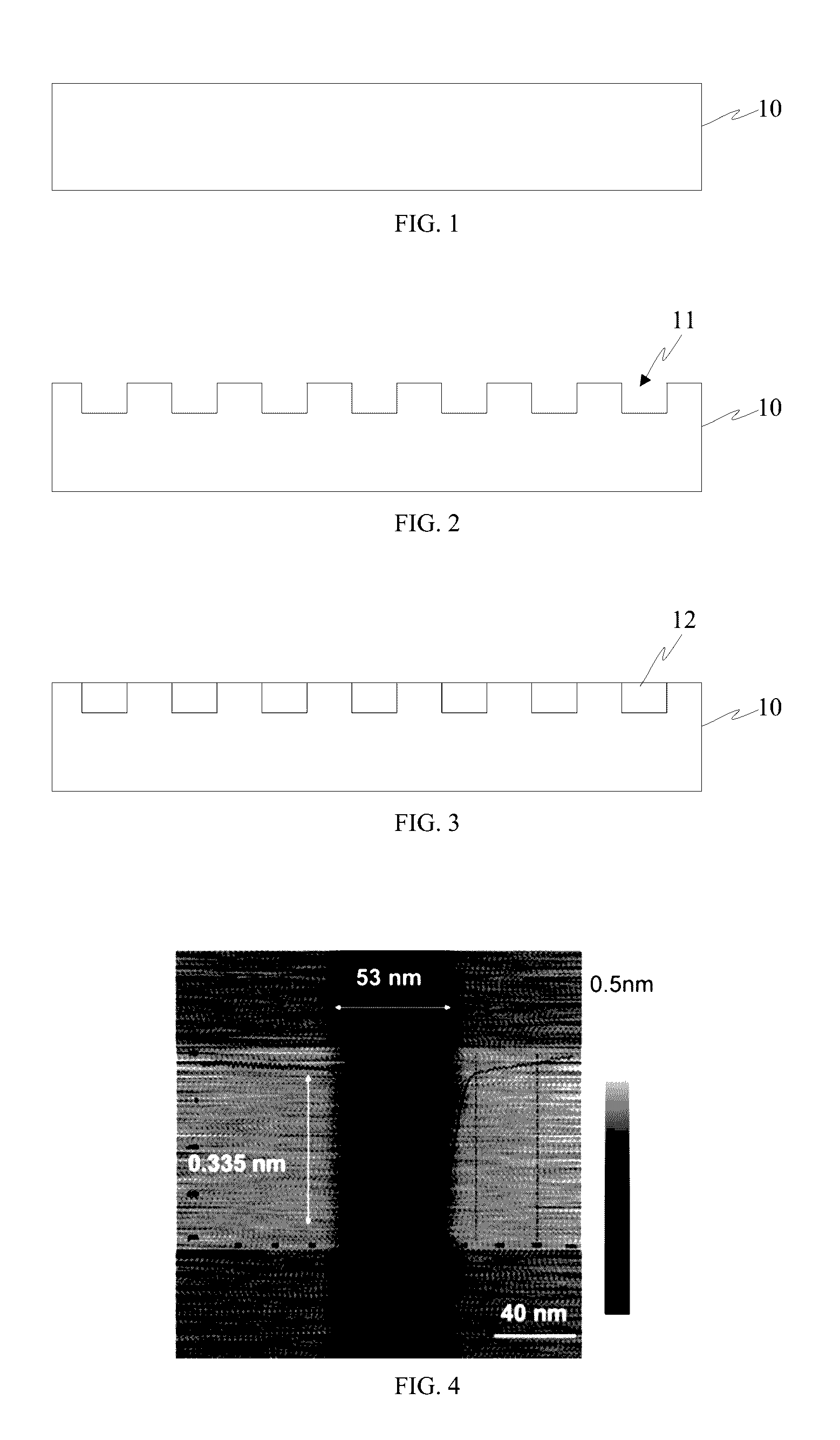
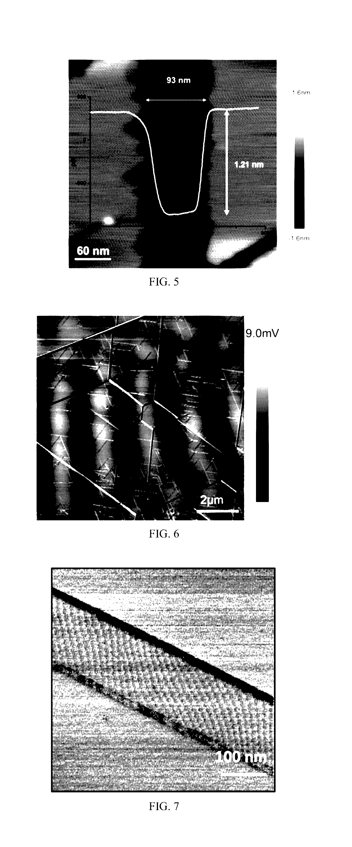
[0045]Please refer to FIG. 1 to FIG. 9. It is to be noted that the drawings provided in the present embodiment only explain the basic conception of the present invention in an illustrative manner, so the drawings only display the components relevant to the present invention rather than being drawn according to the number, shape and size of the components during actual implementation, the shape, numb...


PUM

PropertyMeasurementUnit
widthaaaaaaaaaa
lengthaaaaaaaaaa
thicknessaaaaaaaaaa

Abstract

A preparation method of a graphene nanoribbon on h-BN, comprising: 1) forming a h-BN groove template with a nano ribbon-shaped groove structure on the h-BN by adopting a metal catalysis etching method; 2) growing a graphene nanoribbon in the h-BN groove template by adopting a chemical vapor deposition method. In the present invention, a CVD method is adopted to directly prepare a morphology controllable graphene nanoribbon on the h-BN, which helps to solve the long-term critical problem that the graphene is difficult to nucleate and grow on an insulating substrate, and to avoid the series of problems introduced by the complicated processes of the transferring of the graphene and the subsequent clipping manufacturing for a nanoribbon and the like.

Description

CROSS REFERENCE TO RELATED PATENT APPLICATION[0001]The present application claims the priority of CN 2015100986759 filed on Mar. 5, 2015.BACKGROUND OF THE PRESENT INVENTION[0002]Field of Invention[0003]The present invention belongs to the field of low-dimensional materials and advanced materials, and particularly relates to a preparation method of a graphene nanoribbon on h-BN (hexagonal boron nitride (h-BN)).[0004]Description of Related Arts[0005]Graphene has become a popular research issue in science and industry due to its superior nature in physical-chemical properties, and is expected to be a significant building-block material in the new generation of micro-nano electronic devices due to its superior electronic transport characteristics and clipping manufacturing characteristics. However, the property of the current graphene is subject to the preparation method and means, and the application thereof is thus limited. At present, the commonly used method for preparing a graphene...

Claims


Application Information

Patent Timeline
Patent Type & Authority Patents(United States)
IPC IPC(8): H01L21/02H01L21/311
CPCH01L21/02527H01L21/0259H01L21/02642H01L21/31111C01B2204/06H01L21/02389H01L21/0243H01L21/0262H01L21/02658
Inventor WANG, HAOMINHE, LICHEN, LINGXIUXIE, HONGWANG, HUISHANTANG, SHUJIELI, LEIZHANG, DAOLIXIE, XIAOMINGJIANG, MIANHENG
Owner SHANGHAI INST OF MICROSYSTEM & INFORMATION TECH CHINESE ACAD OF SCI
Why Eureka
Try Eureka